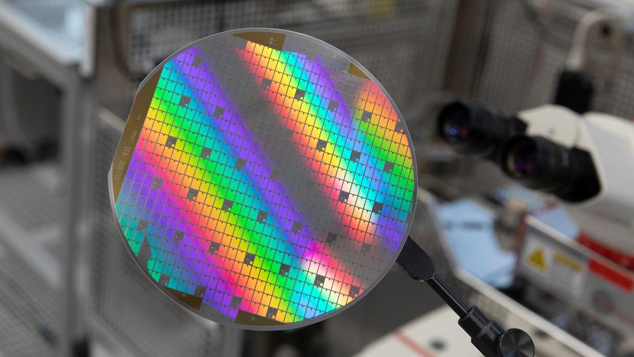
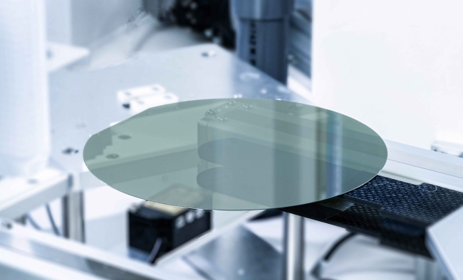
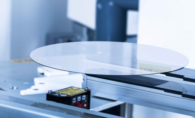
VET Energy silicon carbide (SiC) epitaxial wafer is a high-performance wide bandgap semiconductor material with excellent high temperature resistance, high frequency and high power characteristics. It is an ideal substrate for the new generation of power electronic devices. VET Energy uses advanced MOCVD epitaxial technology to grow high-quality SiC epitaxial layers on SiC substrates, ensuring the excellent performance and consistency of the wafer.
Our Silicon Carbide (SiC) Epitaxial Wafer offers excellent compatibility with a variety of semiconductor materials including Si Wafer, SiC Substrate, SOI Wafer, and SiN Substrate. With its robust epitaxial layer, it supports advanced processes such as Epi Wafer growth and integration with materials like Gallium Oxide Ga2O3 and AlN Wafer, ensuring versatile use across different technologies. Designed to be compatible with industry-standard Cassette handling systems, it ensures efficient and streamlined operations in semiconductor fabrication environments.
VET Energy's product line is not limited to SiC epitaxial wafers. We also provide a wide range of semiconductor substrate materials, including Si Wafer, SiC Substrate, SOI Wafer, SiN Substrate, Epi Wafer, etc. In addition, we are also actively developing new wide bandgap semiconductor materials, such as Gallium Oxide Ga2O3 and AlN Wafer, to meet the future power electronics industry's demand for higher performance devices.
WAFERING SPECIFICATIONS
*n-Pm=n-type Pm-Grade,n-Ps=n-type Ps-Grade,Sl=Semi-lnsulating
|
Item |
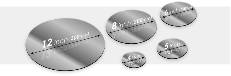
8-Inch |
6-Inch |
4-Inch |
||
|
n-P |
n-Pm |
n-Ps |
SI |
SI |
|
|
TTV(GBIR) |
≤6um |
≤6um |
|||
|
Bow(GF3YFCD)-Absolute Value |
≤15μm |
≤15μm |
≤25μm |
≤15μm |
|
|
Warp(GF3YFER) |
≤25μm |
≤25μm |
≤40μm |
≤25μm |
|
|
LTV(SBIR)-10mmx10mm |
<2μm |
||||
|
Wafer Edge |
Beveling |
||||
SURFACE FINISH
*n-Pm=n-type Pm-Grade,n-Ps=n-type Ps-Grade,Sl=Semi-lnsulating
|
Item |
8-Inch |
6-Inch |
4-Inch |
||
|
n-P |
n-Pm |
n-Ps |
SI |
SI |
|
|
Surface Finish |
Double side Optical Polish,Si- Face CMP |
||||
|
SurfaceRoughness |
(10um x 10um) Si-FaceRa≤0.2nm |
(5umx5um) Si-Face Ra≤0.2nm |
|||
|
Edge Chips |
None Permitted (length and width≥0.5mm) |
||||
|
Indents |
None Permitted |
||||
|
Scratches(Si-Face) |
Qty.≤5,Cumulative |
Qty.≤5,Cumulative |
Qty.≤5,Cumulative |
||
|
Cracks |
None Permitted |
||||
|
Edge Exclusion |
3mm |
||||