In the back-end process stage, the wafer (silicon wafer with circuits on the front) needs to be thinned on the back before subsequent dicing, welding and packaging to reduce the package mounting height, reduce the chip package volume, improve the chip's thermal diffusion efficiency, electrical performance, mechanical properties and reduce the amount of dicing. Back grinding has the advantages of high efficiency and low cost. It has replaced the traditional wet etching and ion etching processes to become the most important back thinning technology.
The thinned wafer
How to thin?
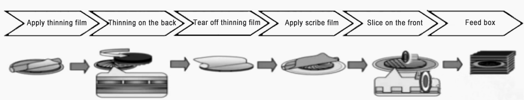
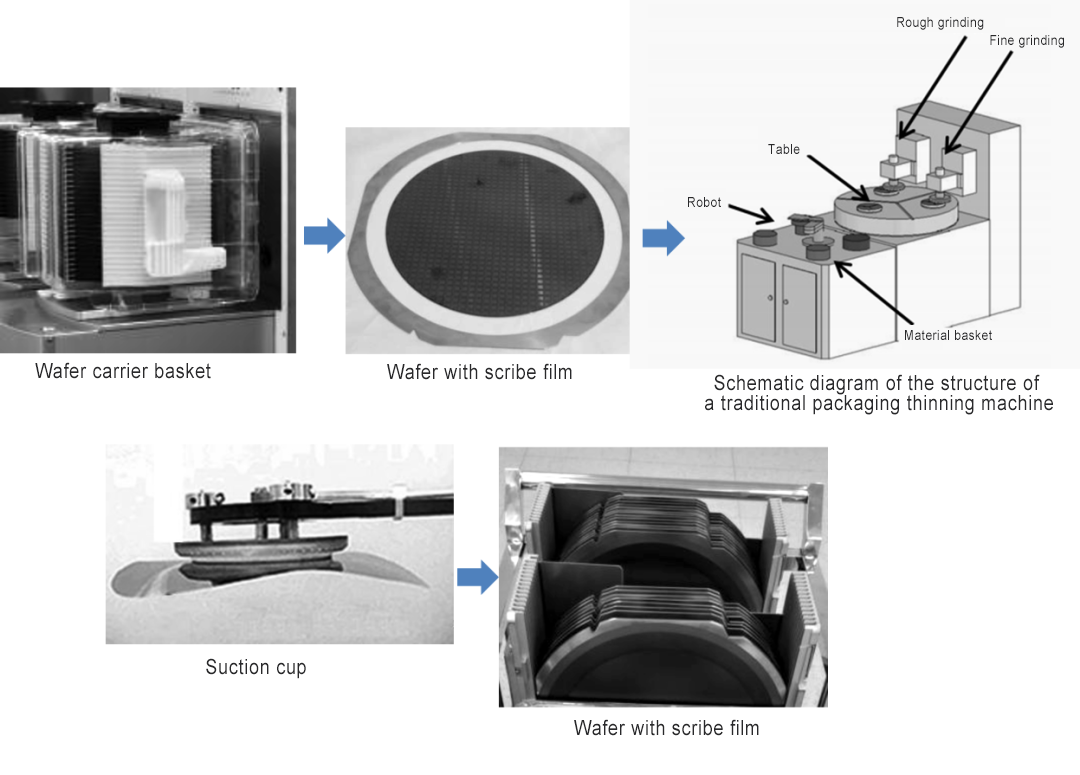 Main process of wafer thinning in traditional packaging process
The specific steps of wafer thinning are to bond the wafer to be processed to the thinning film, and then use vacuum to adsorb the thinning film and the chip on it to the porous ceramic wafer table, adjust the inner and outer circular boat center lines of the working surface of the cup-shaped diamond grinding wheel to the center of the silicon wafer, and the silicon wafer and the grinding wheel rotate around their respective axes for cutting-in grinding. Grinding includes three stages: rough grinding, fine grinding and polishing.
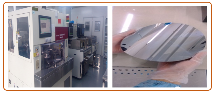
The wafer coming out of the wafer factory is back-grinded to thin the wafer to the thickness required for packaging. When grinding the wafer, tape needs to be applied to the front (Active Area) to protect the circuit area, and the back side is ground at the same time. After grinding, remove the tape and measure the thickness.
The grinding processes that have been successfully applied to silicon wafer preparation include rotary table grinding, silicon wafer rotation grinding, double-sided grinding, etc. With the further improvement of the surface quality requirements of single crystal silicon wafers, new grinding technologies are constantly proposed, such as TAIKO grinding, chemical mechanical grinding, polishing grinding and planetary disc grinding.
Rotary table grinding:
Rotary table grinding (rotary table grinding) is an early grinding process used in silicon wafer preparation and back thinning. Its principle is shown in Figure 1. The silicon wafers are fixed on the suction cups of the rotating table, and rotate synchronously driven by the rotating table. The silicon wafers themselves do not rotate around their axis; the grinding wheel is fed axially while rotating at high speed, and the diameter of the grinding wheel is larger than the diameter of the silicon wafer. There are two types of rotary table grinding: face plunge grinding and face tangential grinding. In face plunge grinding, the grinding wheel width is larger than the silicon wafer diameter, and the grinding wheel spindle feeds continuously along its axial direction until the excess is processed, and then the silicon wafer is rotated under the drive of the rotary table; in face tangential grinding, the grinding wheel feeds along its axial direction, and the silicon wafer is continuously rotated under the drive of the rotating disk, and the grinding is completed by reciprocating feeding (reciprocation) or creep feeding (creepfeed).
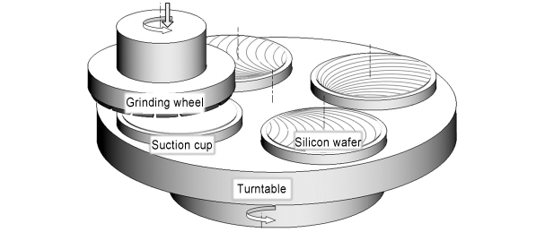
Figure 1, schematic diagram of rotary table grinding (face tangential) principle
Compared with the grinding method, rotary table grinding has the advantages of high removal rate, small surface damage, and easy automation. However, the actual grinding area (active grinding) B and the cut-in angle θ (the angle between the outer circle of the grinding wheel and the outer circle of the silicon wafer) in the grinding process change with the change of the cutting position of the grinding wheel, resulting in an unstable grinding force, making it difficult to obtain the ideal surface accuracy (high TTV value), and easily causing defects such as edge collapse and edge collapse. The rotary table grinding technology is mainly used for the processing of single-crystal silicon wafers below 200mm. The increase in the size of single-crystal silicon wafers has put forward higher requirements for the surface accuracy and motion accuracy of the equipment workbench, so the rotary table grinding is not suitable for the grinding of single-crystal silicon wafers above 300mm.
In order to improve the grinding efficiency, commercial plane tangential grinding equipment usually adopts a multi-grinding wheel structure. For example, a set of rough grinding wheels and a set of fine grinding wheels are equipped on the equipment, and the rotary table rotates one circle to complete the rough grinding and fine grinding in turn. This type of equipment includes the G-500DS of the American GTI Company (Figure 2).
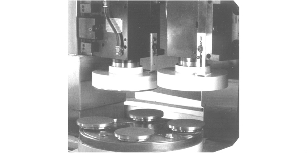
Figure 2, G-500DS rotary table grinding equipment of GTI Company in the United States
Silicon wafer rotation grinding:
In order to meet the needs of large-size silicon wafer preparation and back thinning processing, and obtain surface accuracy with good TTV value. In 1988, Japanese scholar Matsui proposed a silicon wafer rotation grinding (in-feedgrinding) method. Its principle is shown in Figure 3. The single crystal silicon wafer and cup-shaped diamond grinding wheel adsorbed on the workbench rotate around their respective axes, and the grinding wheel is continuously fed along the axial direction at the same time. Among them, the diameter of the grinding wheel is larger than the diameter of the processed silicon wafer, and its circumference passes through the center of the silicon wafer. In order to reduce the grinding force and reduce the grinding heat, the vacuum suction cup is usually trimmed into a convex or concave shape or the angle between the grinding wheel spindle and the suction cup spindle axis is adjusted to ensure semi-contact grinding between the grinding wheel and the silicon wafer.
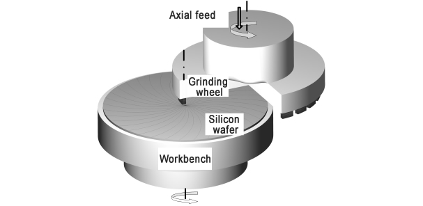
Figure 3, Schematic diagram of silicon wafer rotary grinding principle
Compared with rotary table grinding, silicon wafer rotary grinding has the following advantages: ① Single-time single-wafer grinding can process large-size silicon wafers over 300mm; ② The actual grinding area B and the cutting angle θ are constant, and the grinding force is relatively stable; ③ By adjusting the inclination angle between the grinding wheel axis and the silicon wafer axis, the surface shape of the single crystal silicon wafer can be actively controlled to obtain better surface shape accuracy. In addition, the grinding area and cutting angle θ of silicon wafer rotary grinding also have the advantages of large margin grinding, easy online thickness and surface quality detection and control, compact equipment structure, easy multi-station integrated grinding, and high grinding efficiency.
In order to improve production efficiency and meet the needs of semiconductor production lines, commercial grinding equipment based on the principle of silicon wafer rotary grinding adopts a multi-spindle multi-station structure, which can complete rough grinding and fine grinding in one loading and unloading. Combined with other auxiliary facilities, it can realize the fully automatic grinding of single crystal silicon wafers "dry-in/dry-out" and "cassette to cassette".
Double-sided grinding:
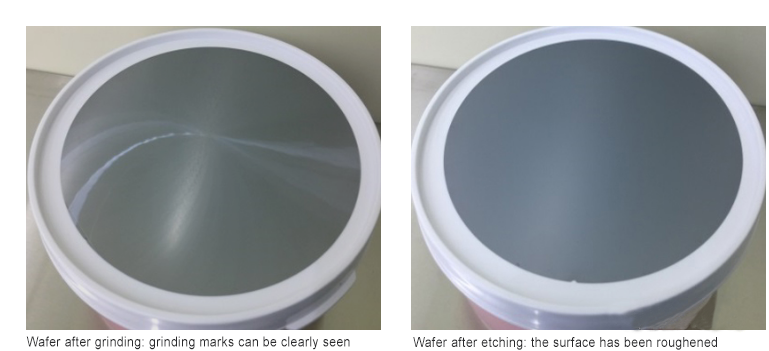
When the silicon wafer rotary grinding processes the upper and lower surfaces of the silicon wafer, the workpiece needs to be turned over and carried out in steps, which limits the efficiency. At the same time, the silicon wafer rotary grinding has surface error copying (copied) and grinding marks (grindingmark), and it is impossible to effectively remove the defects such as waviness and taper on the surface of the single crystal silicon wafer after wire cutting (multi-saw), as shown in Figure 4. To overcome the above defects, double-sided grinding technology (doublesidegrinding) appeared in the 1990s, and its principle is shown in Figure 5. The clamps symmetrically distributed on both sides clamp the single crystal silicon wafer in the retaining ring and rotate slowly driven by the roller. A pair of cup-shaped diamond grinding wheels are relatively located on both sides of the single crystal silicon wafer. Driven by the air bearing electric spindle, they rotate in opposite directions and feed axially to achieve double-sided grinding of the single crystal silicon wafer. As can be seen from the figure, double-sided grinding can effectively remove the waviness and taper on the surface of the single crystal silicon wafer after wire cutting. According to the arrangement direction of the grinding wheel axis, double-sided grinding can be horizontal and vertical. Among them, horizontal double-sided grinding can effectively reduce the influence of silicon wafer deformation caused by the dead weight of the silicon wafer on the grinding quality, and it is easy to ensure that the grinding process conditions on both sides of the single crystal silicon wafer are the same, and the abrasive particles and grinding chips are not easy to stay on the surface of the single crystal silicon wafer. It is a relatively ideal grinding method.
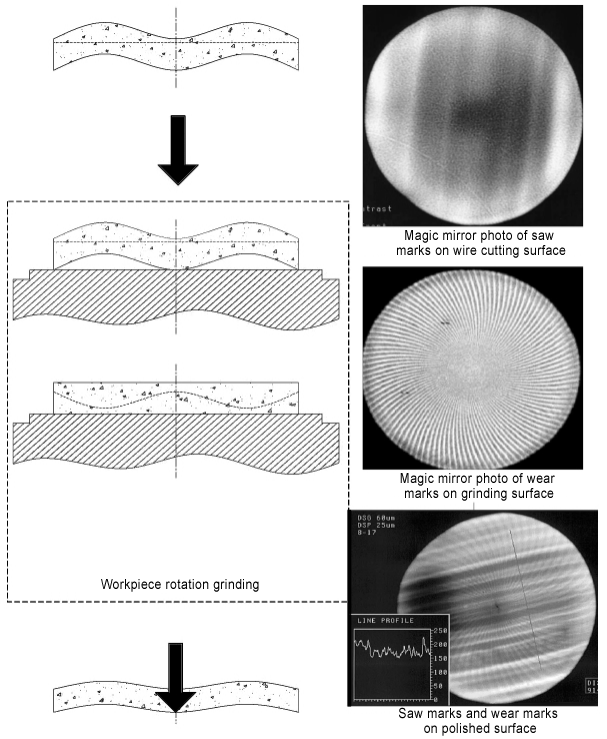
Figure 4, "Error copy" and wear mark defects in silicon wafer rotation grinding
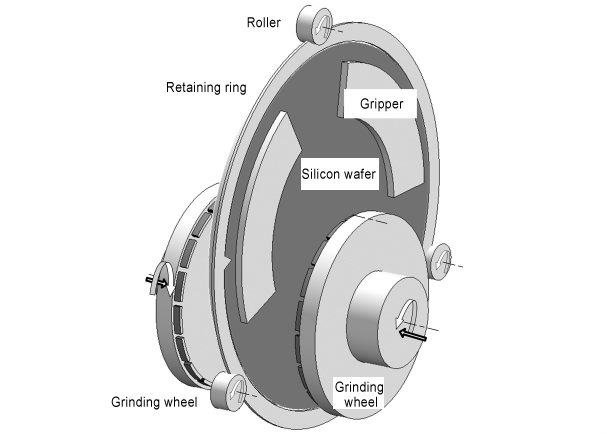
Figure 5, schematic diagram of double-sided grinding principle
Table 1 shows the comparison between the grinding and double-sided grinding of the above three types of single crystal silicon wafers. Double-sided grinding is mainly used for silicon wafer processing below 200mm, and has a high wafer yield. Due to the use of fixed abrasive grinding wheels, the grinding of single-crystal silicon wafers can obtain a much higher surface quality than that of double-sided grinding. Therefore, both silicon wafer rotary grinding and double-sided grinding can meet the processing quality requirements of mainstream 300mm silicon wafers, and are currently the most important flattening processing methods. When selecting a silicon wafer flattening processing method, it is necessary to comprehensively consider the requirements of the diameter size, surface quality, and polishing wafer processing technology of the single-crystal silicon wafer. The back thinning of the wafer can only select a single-sided processing method, such as the silicon wafer rotary grinding method.
In addition to selecting the grinding method in silicon wafer grinding, it is also necessary to determine the selection of reasonable process parameters such as positive pressure, grinding wheel grain size, grinding wheel binder, grinding wheel speed, silicon wafer speed, grinding fluid viscosity and flow rate, etc., and determine a reasonable process route. Usually, a segmented grinding process including rough grinding, semi-finishing grinding, finishing grinding, spark-free grinding and slow backing is used to obtain single crystal silicon wafers with high processing efficiency, high surface flatness and low surface damage.
New grinding technology can refer to the literature:
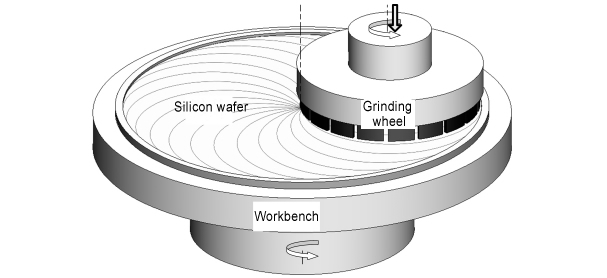
Figure 5, schematic diagram of TAIKO grinding principle
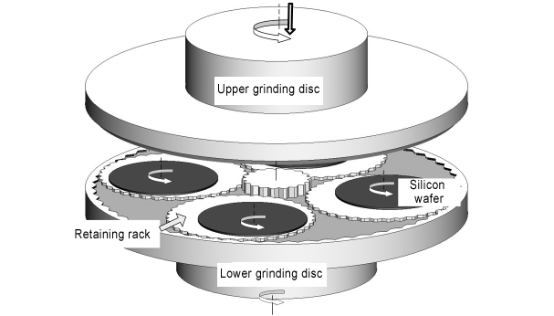
Figure 6, schematic diagram of planetary disk grinding principle
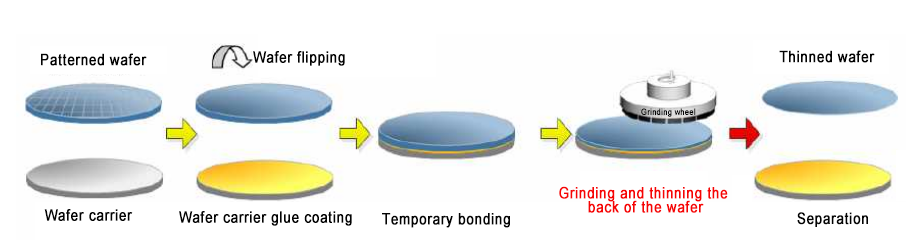
Ultra-thin wafer grinding thinning technology:
There are wafer carrier grinding thinning technology and edge grinding technology (Figure 5).
Post time: Aug-08-2024