A wafer has to go through three changes to become a real semiconductor chip: first, the block-shaped ingot is cut into wafers; in the second process, transistors are engraved on the front of the wafer through the previous process; finally, packaging is performed, that is, through the cutting process, the wafer becomes a complete semiconductor chip. It can be seen that the packaging process belongs to the back-end process. In this process, the wafer will be cut into several hexahedron individual chips. This process of obtaining independent chips is called “Singulation”, and the process of sawing the wafer board into independent cuboids is called “wafer cutting (Die Sawing)”. Recently, with the improvement of semiconductor integration, the thickness of wafers has become thinner and thinner, which of course brings a lot of difficulty to the “singulation” process.
The evolution of wafer dicing
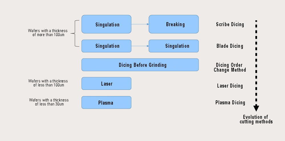
Front-end and back-end processes have evolved through interaction in various ways: the evolution of back-end processes can determine the structure and position of the hexahedron small chips separated from the die on the wafer, as well as the structure and position of the pads (electrical connection paths) on the wafer; on the contrary, the evolution of front-end processes has changed the process and method of wafer back thinning and “die dicing” in the back-end process. Therefore, the increasingly sophisticated appearance of the package will have a great impact on the back-end process. Moreover, the number, procedure and type of dicing will also change accordingly according to the change in the appearance of the package.
Scribe Dicing
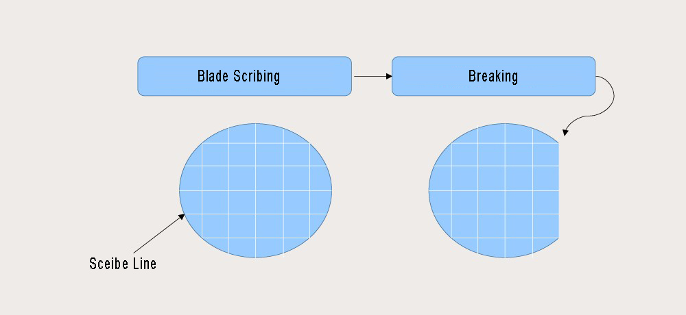
In the early days, “breaking” by applying external force was the only dicing method that could divide the wafer into hexahedron dies. However, this method has the disadvantages of chipping or cracking of the edge of the small chip. In addition, since the burrs on the metal surface are not completely removed, the cut surface is also very rough.
In order to solve this problem, the “Scribing” cutting method came into being, that is, before “breaking”, the surface of the wafer is cut to about half the depth. “Scribing”, as the name suggests, refers to using an impeller to saw (half-cut) the front side of the wafer in advance. In the early days, most wafers below 6 inches used this cutting method of first “slicing” between chips and then “breaking”.
Blade Dicing or Blade Sawing
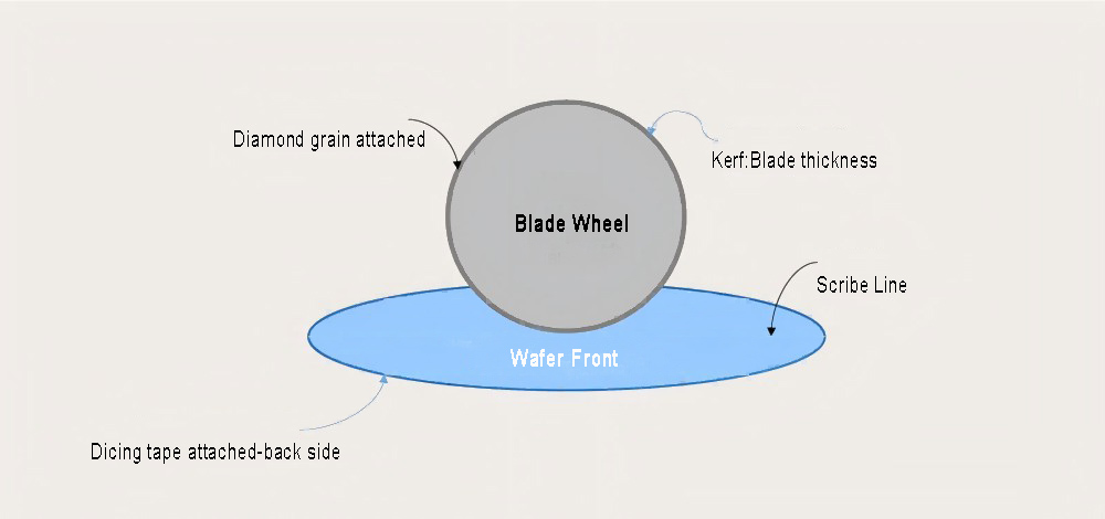
The “Scribing” cutting method gradually developed into the “Blade dicing” cutting (or sawing) method, which is a method of cutting using a blade two or three times in a row. The “Blade” cutting method can make up for the phenomenon of small chips peeling off when “breaking” after “scribing”, and can protect small chips during the “singulation” process. “Blade” cutting is different from the previous “dicing” cutting, that is, after a “blade” cutting, it is not “breaking”, but cutting again with a blade. Therefore, it is also called “step dicing” method.
In order to protect the wafer from external damage during the cutting process, a film will be applied to the wafer in advance to ensure safer “singling”. During the “back grinding” process, the film will be attached to the front of the wafer. But on the contrary, in “blade” cutting, the film should be attached to the back of the wafer. During the eutectic die bonding (die bonding, fixing the separated chips on the PCB or fixed frame), the film attached to the back will automatically fall off. Due to the high friction during cutting, DI water should be sprayed continuously from all directions. In addition, the impeller should be attached with diamond particles so that the slices can be sliced better. At this time, the cut (blade thickness: groove width) must be uniform and must not exceed the width of the dicing groove.
For a long time, sawing has been the most widely used traditional cutting method. Its biggest advantage is that it can cut a large number of wafers in a short time. However, if the feeding speed of the slice is greatly increased, the possibility of chiplet edge peeling will increase. Therefore, the number of rotations of the impeller should be controlled at about 30,000 times per minute. It can be seen that the technology of semiconductor process is often a secret accumulated slowly through a long period of accumulation and trial and error (in the next section on eutectic bonding, we will discuss the content about cutting and DAF).
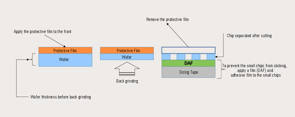
Dicing before grinding (DBG): the cutting sequence has changed the method
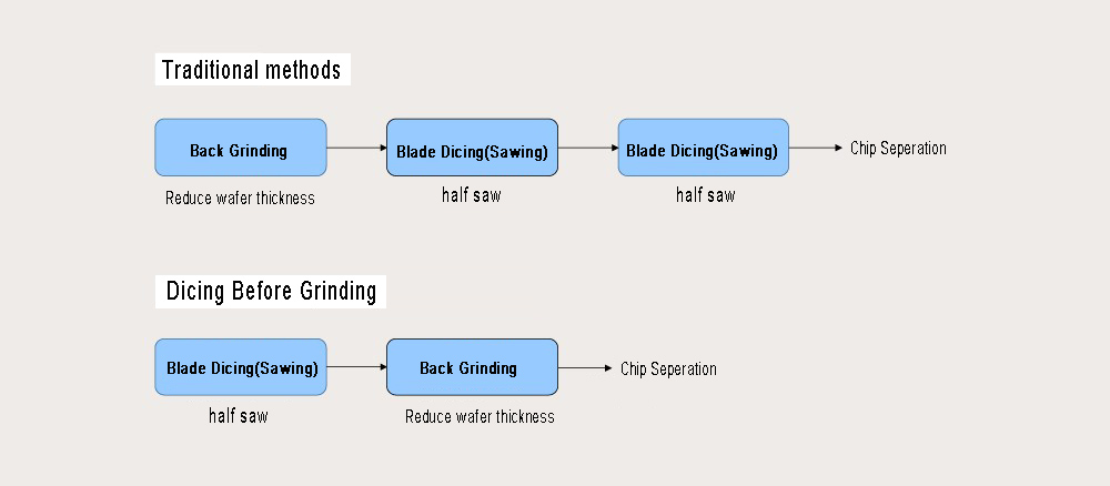
When blade cutting is performed on an 8-inch diameter wafer, there is no need to worry about chiplet edge peeling or cracking. But as the wafer diameter increases to 21 inches and the thickness becomes extremely thin, peeling and cracking phenomena begin to appear again. In order to significantly reduce the physical impact on the wafer during the cutting process, the DBG method of “dicing before grinding” replaces the traditional cutting sequence. Unlike the traditional “blade” cutting method that cuts continuously, DBG first performs a “blade” cut, and then gradually thins the wafer thickness by continuously thinning the back side until the chip is split. It can be said that DBG is an upgraded version of the previous “blade” cutting method. Because it can reduce the impact of the second cut, the DBG method has been rapidly popularized in “wafer-level packaging”.
Laser Dicing
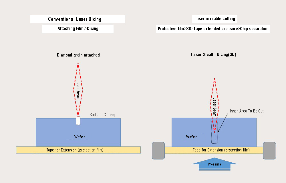
The wafer-level chip scale package (WLCSP) process mainly uses laser cutting. Laser cutting can reduce phenomena such as peeling and cracking, thereby obtaining better quality chips, but when the wafer thickness is more than 100μm, the productivity will be greatly reduced. Therefore, it is mostly used on wafers with a thickness of less than 100μm (relatively thin). Laser cutting cuts silicon by applying high-energy laser to the wafer’s scribe groove. However, when using the conventional laser (Conventional Laser) cutting method, a protective film must be applied to the wafer surface in advance. Because heating or irradiating the surface of the wafer with laser, these physical contacts will produce grooves on the surface of the wafer, and the cut silicon fragments will also adhere to the surface. It can be seen that the traditional laser cutting method also directly cuts the surface of the wafer, and in this respect, it is similar to the “blade” cutting method.
Stealth Dicing (SD) is a method of first cutting the inside of the wafer with laser energy, and then applying external pressure to the tape attached to the back to break it, thereby separating the chip. When pressure is applied to the tape on the back, the wafer will be instantly raised upward due to the stretching of the tape, thereby separating the chip. The advantages of SD over the traditional laser cutting method are: first, there is no silicon debris; second, the kerf (Kerf: the width of the scribe groove) is narrow, so more chips can be obtained. In addition, the peeling and cracking phenomenon will be greatly reduced using the SD method, which is crucial to the overall quality of the cutting. Therefore, the SD method is very likely to become the most popular technology in the future.
Plasma Dicing
Plasma cutting is a recently developed technology that uses plasma etching to cut during the manufacturing (Fab) process. Plasma cutting uses semi-gas materials instead of liquids, so the impact on the environment is relatively small. And the method of cutting the entire wafer at one time is adopted, so the “cutting” speed is relatively fast. However, the plasma method uses chemical reaction gas as raw material, and the etching process is very complicated, so its process flow is relatively cumbersome. But compared with “blade” cutting and laser cutting, plasma cutting does not cause damage to the wafer surface, thereby reducing the defect rate and obtaining more chips.
Recently, since the wafer thickness has been reduced to 30μm, and a lot of copper (Cu) or low dielectric constant materials (Low-k) are used. Therefore, in order to prevent burrs (Burr), plasma cutting methods will also be favored. Of course, plasma cutting technology is also constantly developing. I believe that in the near future, one day there will be no need to wear a special mask when etching, because this is a major development direction of plasma cutting.
As the thickness of wafers has been continuously reduced from 100μm to 50μm and then to 30μm, the cutting methods for obtaining independent chips have also been changing and developing from “breaking” and “blade” cutting to laser cutting and plasma cutting. Although the increasingly mature cutting methods have increased the production cost of the cutting process itself, on the other hand, by significantly reducing the undesirable phenomena such as peeling and cracking that often occur in semiconductor chip cutting and increasing the number of chips obtained per unit wafer, the production cost of a single chip has shown a downward trend. Of course, the increase in the number of chips obtained per unit area of the wafer is closely related to the reduction in the width of the dicing street. Using plasma cutting, nearly 20% more chips can be obtained compared to using the “blade” cutting method, which is also a major reason why people choose plasma cutting. With the development and changes of wafers, chip appearance and packaging methods, various cutting processes such as wafer processing technology and DBG are also emerging.
Post time: Oct-10-2024