The technical difficulties in stably mass-producing high-quality silicon carbide wafers with stable performance include:
1) Since crystals need to grow in a high-temperature sealed environment above 2000°C, the temperature control requirements are extremely high;
2) Since silicon carbide has more than 200 crystal structures, but only a few structures of single-crystal silicon carbide are the required semiconductor materials, the silicon-to-carbon ratio, growth temperature gradient, and crystal growth need to be precisely controlled during the crystal growth process. Parameters such as speed and air flow pressure;
3) Under the vapor phase transmission method, the diameter expansion technology of silicon carbide crystal growth is extremely difficult;
4) The hardness of silicon carbide is close to that of diamond, and cutting, grinding, and polishing techniques are difficult.
SiC epitaxial wafers: usually manufactured by chemical vapor deposition (CVD) method. According to different doping types, they are divided into n-type and p-type epitaxial wafers. Domestic Hantian Tiancheng and Dongguan Tianyu can already provide 4-inch/6-inch SiC epitaxial wafers. For SiC epitaxy, it is difficult to control in the high-voltage field, and the quality of SiC epitaxy has a greater impact on SiC devices. Moreover, epitaxial equipment is monopolized by the four leading companies in the industry: Axitron, LPE, TEL and Nuflare.
Silicon carbide epitaxial wafer refers to a silicon carbide wafer in which a single crystal film (epitaxial layer) with certain requirements and the same as the substrate crystal is grown on the original silicon carbide substrate. Epitaxial growth mainly uses CVD (Chemical Vapor Deposition, ) equipment or MBE (Molecular Beam Epitaxy) equipment. Since silicon carbide devices are manufactured directly in the epitaxial layer, the quality of the epitaxial layer directly affects the performance and yield of the device. As the voltage withstand performance of the device continues to increase, the thickness of the corresponding epitaxial layer becomes thicker and the control becomes more difficult.Generally, when the voltage is around 600V, the required epitaxial layer thickness is about 6 microns; when the voltage is between 1200-1700V, the required epitaxial layer thickness reaches 10-15 microns. If the voltage reaches more than 10,000 volts, an epitaxial layer thickness of more than 100 microns may be required. As the thickness of the epitaxial layer continues to increase, it becomes increasingly difficult to control thickness and resistivity uniformity and defect density.
SiC devices: Internationally, 600~1700V SiC SBD and MOSFET have been industrialized. The mainstream products operate at voltage levels below 1200V and primarily adopt TO packaging. In terms of pricing, SiC products on the international market are priced at around 5-6 times higher than their Si counterparts. However, prices are decreasing at an annual rate of 10%. with the expansion of upstream materials and device production in the next 2-3 years, the market supply will increase, leading to further price reductions. It is expected that when the price reaches 2-3 times that of Si products, the advantages brought by reduced system costs and improved performance will gradually drive SiC to occupy the market space of Si devices.
Traditional packaging is based on silicon-based substrates, while third-generation semiconductor materials require a completely new design. Using traditional silicon-based packaging structures for wide-bandgap power devices can introduce new issues and challenges related to frequency, thermal management, and reliability. SiC power devices are more sensitive to parasitic capacitance and inductance. Compared to Si devices, SiC power chips have faster switching speeds, which can lead to overshoot, oscillation, increased switching losses, and even device malfunctions. Additionally, SiC power devices operate at higher temperatures, requiring more advanced thermal management techniques.
A variety of different structures have been developed in the field of wide-bandgap semiconductor power packaging. Traditional Si-based power module packaging is no longer suitable. In order to solve the problems of high parasitic parameters and poor heat dissipation efficiency of traditional Si-based power module packaging, SiC power module packaging adopts wireless interconnection and double-side cooling technology in its structure, and also adopts the substrate materials with better thermal conductivity, and tried to integrate decoupling capacitors, temperature/current sensors, and drive circuits into the module structure, and developed a variety of different module packaging technologies. Moreover, there are high technical barriers to SiC device manufacturing and production costs are high.
Silicon carbide devices are produced by depositing epitaxial layers on a silicon carbide substrate through CVD. The process involves cleaning, oxidation, photolithography, etching, stripping of photoresist, ion implantation, chemical vapor deposition of silicon nitride, polishing, sputtering, and subsequent processing steps to form the device structure on the SiC single crystal substrate. Main types of SiC power devices include SiC diodes, SiC transistors, and SiC power modules. Due to factors such as slow upstream material production speed and low yield rates, silicon carbide devices have relatively high manufacturing costs.
In addition, silicon carbide device manufacturing has certain technical difficulties:
1) It is necessary to develop a specific process that is consistent with the characteristics of silicon carbide materials. For example: SiC has a high melting point, which makes traditional thermal diffusion ineffective. It is necessary to use ion implantation doping method and accurately control parameters such as temperature, heating rate, duration, and gas flow; SiC is inert to chemical solvents. Methods such as dry etching should be used, and mask materials, gas mixtures, control of sidewall slope, etching rate, sidewall roughness, etc. should be optimized and developed;
2) The manufacturing of metal electrodes on silicon carbide wafers requires contact resistance below 10-5Ω2. The electrode materials that meet the requirements, Ni and Al, have poor thermal stability above 100°C, but Al/Ni has better thermal stability. The contact specific resistance of /W/Au composite electrode material is 10-3Ω2 higher;
3) SiC has high cutting wear, and the hardness of SiC is second only to diamond, which puts forward higher requirements for cutting, grinding, polishing and other technologies.
Moreover, trench silicon carbide power devices are more difficult to manufacture. According to different device structures, silicon carbide power devices can be mainly divided into planar devices and trench devices. Planar silicon carbide power devices have good unit consistency and simple manufacturing process, but are prone to JFET effect and have high parasitic capacitance and on-state resistance. Compared with planar devices, trench silicon carbide power devices have lower unit consistency and have a more complex manufacturing process. However, the trench structure is conducive to increasing the device unit density and is less likely to produce the JFET effect, which is beneficial to solving the problem of channel mobility. It has excellent properties such as small on-resistance, small parasitic capacitance, and low switching energy consumption. It has significant cost and performance advantages and has become the mainstream direction of the development of silicon carbide power devices. According to Rohm official website, the ROHM Gen3 structure (Gen1 Trench structure) is only 75% of the Gen2 (Plannar2) chip area, and the ROHM Gen3 structure’s on-resistance is reduced by 50% under the same chip size.
Silicon carbide substrate, epitaxy, front-end, R&D expenses and others account for 47%, 23%, 19%, 6% and 5% of the manufacturing cost of silicon carbide devices respectively.
Finally, we will focus on breaking down the technical barriers of substrates in the silicon carbide industry chain.
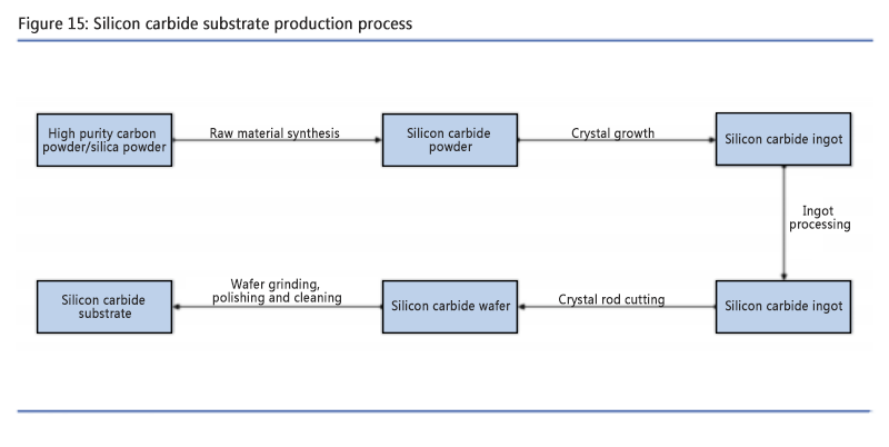
The production process of silicon carbide substrates is similar to that of silicon-based substrates, but more difficult.
The manufacturing process of silicon carbide substrate generally includes raw material synthesis, crystal growth, ingot processing, ingot cutting, wafer grinding, polishing, cleaning and other links.
The crystal growth stage is the core of the entire process, and this step determines the electrical properties of the silicon carbide substrate.
Silicon carbide materials are difficult to grow in the liquid phase under normal conditions. The vapor phase growth method popular in the market today has a growth temperature above 2300°C and requires precise control of the growth temperature. The entire operation process is almost difficult to observe. A slight error will lead to product scrapping. In comparison, silicon materials only require 1600℃, which is much lower. Preparing silicon carbide substrates also faces difficulties such as slow crystal growth and high crystal form requirements. Silicon carbide wafer growth takes about 7 to 10 days, while silicon rod pulling only takes 2 and a half days. Moreover, silicon carbide is a material whose hardness is second only to diamond. It will lose a lot during cutting, grinding, and polishing, and the output ratio is only 60%.
We know that the trend is to increase the size of silicon carbide substrates, as the size continues to increase, the requirements for diameter expansion technology are becoming higher and higher. It requires a combination of various technical control elements to achieve iterative growth of crystals.
Post time: May-22-2024