The first generation of semiconductor materials is represented by traditional silicon (Si) and germanium (Ge), which are the basis for integrated circuit manufacturing. They are widely used in low-voltage, low-frequency, and low-power transistors and detectors. More than 90% of semiconductor products are Made of silicon-based materials;
The second generation semiconductor materials are represented by gallium arsenide (GaAs), indium phosphide (InP) and gallium phosphide (GaP). Compared with silicon-based devices, they have high-frequency and high-speed optoelectronic properties and are widely used in the fields of optoelectronics and microelectronics. ;
The third generation of semiconductor materials is represented by emerging materials such as silicon carbide (SiC), gallium nitride (GaN), zinc oxide (ZnO), diamond (C), and aluminum nitride (AlN).
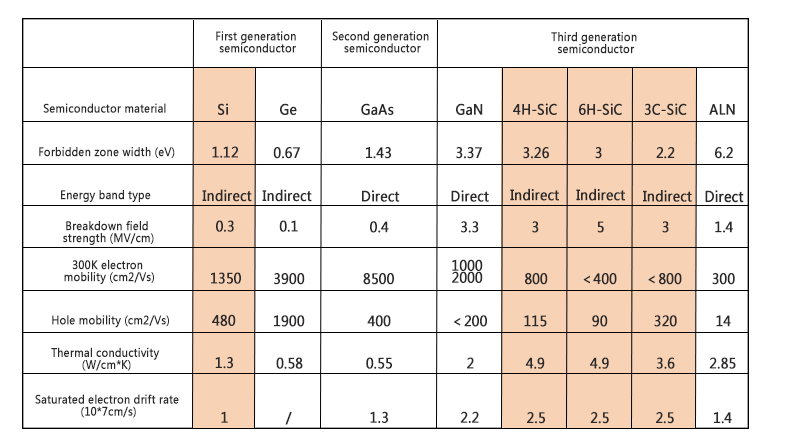
Silicon carbide is an important basic material for the development of the third-generation semiconductor industry. Silicon carbide power devices can effectively meet the high efficiency, miniaturization and lightweight requirements of power electronic systems with their excellent high-voltage resistance, high temperature resistance, low loss and other properties.
Because of its superior physical properties: high band gap (corresponding to high breakdown electric field and high power density), high electrical conductivity, and high thermal conductivity, it is expected to become the most widely used basic material for making semiconductor chips in the future. Especially in the fields of new energy vehicles, photovoltaic power generation, rail transit, smart grids and other fields, it has obvious advantages.
The SiC production process is divided into three major steps: SiC single crystal growth, epitaxial layer growth and device manufacturing, which correspond to the four major links of the industrial chain: substrate, epitaxy, devices and modules.
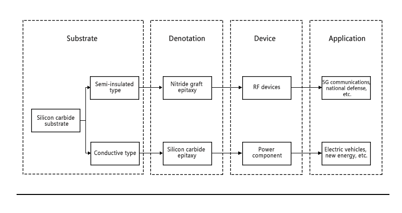
The mainstream method of manufacturing substrates first uses the physical vapor sublimation method to sublimate the powder in a high-temperature vacuum environment, and grow silicon carbide crystals on the surface of the seed crystal through the control of a temperature field. Using a silicon carbide wafer as a substrate, chemical vapor deposition is used to deposit a layer of single crystal on the wafer to form an epitaxial wafer. Among them, growing a silicon carbide epitaxial layer on a conductive silicon carbide substrate can be made into power devices, which are mainly used in electric vehicles, photovoltaics and other fields; growing a gallium nitride epitaxial layer on a semi-insulating silicon carbide substrate can further made into radio frequency devices, used in 5G communications and other fields.
For now, silicon carbide substrates have the highest technical barriers in the silicon carbide industry chain, and silicon carbide substrates are the most difficult to produce.
The production bottleneck of SiC has not been completely solved, and the quality of the raw material crystal pillars is unstable and there is a yield problem, which leads to the high cost of SiC devices. It only takes an average of 3 days for silicon material to grow into a crystal rod, but it takes a week for a silicon carbide crystal rod. A general silicon crystal rod can grow 200cm long, but a silicon carbide crystal rod can only grow 2cm long. Moreover, SiC itself is a hard and brittle material, and wafers made of it are prone to edge chipping when using traditional mechanical cutting wafer dicing, which affects product yield and reliability. SiC substrates are very different from traditional silicon ingots, and everything from equipment, processes, processing to cutting needs to be developed to handle silicon carbide.
The silicon carbide industry chain is mainly divided into four major links: substrate, epitaxy, devices and applications. Substrate materials are the foundation of the industry chain, epitaxial materials are the key to device manufacturing, devices are the core of the industry chain, and applications are the driving force for industrial development. The upstream industry uses raw materials to make substrate materials through physical vapor sublimation methods and other methods, and then uses chemical vapor deposition methods and other methods to grow epitaxial materials. The midstream industry uses upstream materials to make radio frequency devices, power devices and other devices, which are ultimately used in downstream 5G communications. , electric vehicles, rail transit, etc. Among them, substrate and epitaxy account for 60% of the cost of the industry chain and are the main value of the industry chain.
SiC substrate: SiC crystals are usually manufactured using the Lely method. International mainstream products are transitioning from 4 inches to 6 inches, and 8-inch conductive substrate products have been developed. Domestic substrates are mainly 4 inches. Since the existing 6-inch silicon wafer production lines can be upgraded and transformed to produce SiC devices, the high market share of 6-inch SiC substrates will be maintained for a long time.
The silicon carbide substrate process is complex and difficult to produce. Silicon carbide substrate is a compound semiconductor single crystal material composed of two elements: carbon and silicon. At present, the industry mainly uses high-purity carbon powder and high-purity silicon powder as raw materials to synthesize silicon carbide powder. Under a special temperature field, the mature physical vapor transmission method (PVT method) is used to grow silicon carbide of different sizes in a crystal growth furnace. The crystal ingot is finally processed, cut, ground, polished, cleaned and other multiple processes to produce a silicon carbide substrate.
Post time: May-22-2024