The core technology for the growth of SiC epitaxial materials is firstly defect control technology, especially for defect control technology that is prone to device failure or reliability degradation. The study of the mechanism of substrate defects extending into the epitaxial layer during the epitaxial growth process, the transfer and transformation laws of defects at the interface between the substrate and epitaxial layer, and the nucleation mechanism of defects are the basis for clarifying the correlation between substrate defects and epitaxial structural defects, which can effectively guide substrate screening and epitaxial process optimization.
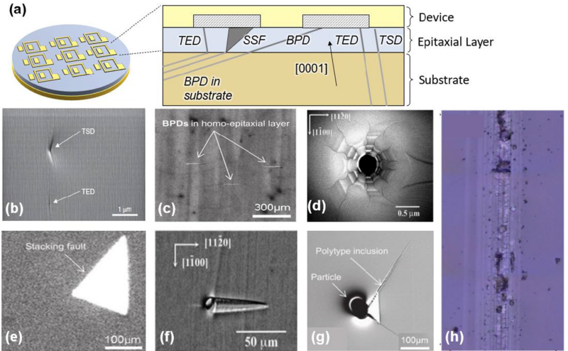
The defects of silicon carbide epitaxial layers are mainly divided into two categories: crystal defects and surface morphology defects. Crystal defects, including point defects, screw dislocations, microtubule defects, edge dislocations, etc., mostly originate from defects on SiC substrates and diffuse into the epitaxial layer. Surface morphology defects can be directly observed with the naked eye using a microscope and have typical morphological characteristics. Surface morphology defects mainly include: Scratch, Triangular defect, Carrot defect, Downfall, and Particle, as shown in Figure 4. During the epitaxial process, foreign particles, substrate defects, surface damage, and epitaxial process deviations may all affect the local step flow growth mode, resulting in surface morphology defects.
Table 1. Causes for the formation of common matrix defects and surface morphology defects in SiC epitaxial layers
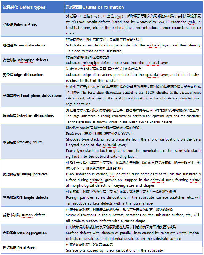
Point defects
Point defects are formed by vacancies or gaps at a single lattice point or several lattice points, and they have no spatial extension. Point defects may occur in every production process, especially in ion implantation. However, they are difficult to detect, and the relationship between the transformation of point defects and other defects is also quite complex.
Micropipes (MP)
Micropipes are hollow screw dislocations that propagate along the growth axis, with a Burgers vector <0001>. The diameter of microtubes ranges from a fraction of a micron to tens of microns. Microtubes show large pit-like surface features on the surface of SiC wafers. Typically, the density of microtubes is about 0.1~1cm-2 and continues to decrease in commercial wafer production quality monitoring.
Screw dislocations (TSD) and edge dislocations (TED)
Dislocations in SiC are the main source of device degradation and failure. Both screw dislocations (TSD) and edge dislocations (TED) run along the growth axis, with Burgers vectors of <0001> and 1/3<11–20>, respectively.
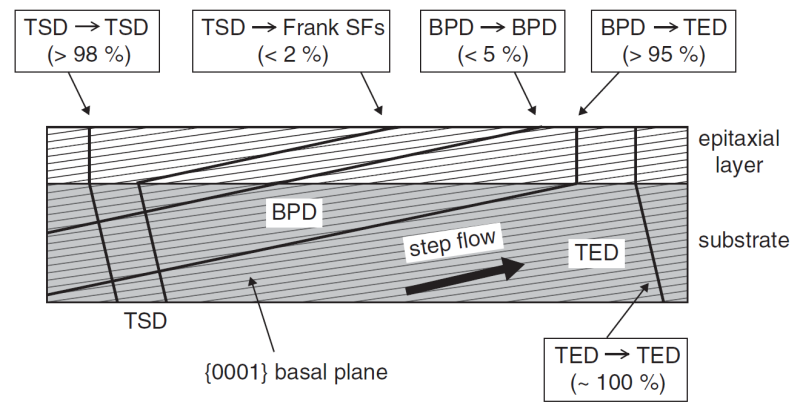
Both screw dislocations (TSD) and edge dislocations (TED) can extend from the substrate to the wafer surface and bring small pit-like surface features (Figure 4b). Typically, the density of edge dislocations is about 10 times that of screw dislocations. Extended screw dislocations, that is, extending from the substrate to the epilayer, may also transform into other defects and propagate along the growth axis. During SiC epitaxial growth, screw dislocations are converted into stacking faults (SF) or carrot defects, while edge dislocations in epilayers are shown to be converted from basal plane dislocations (BPDs) inherited from the substrate during epitaxial growth.
Basic plane dislocation (BPD)
Located on the SiC basal plane, with a Burgers vector of 1/3 <11–20>. BPDs rarely appear on the surface of SiC wafers. They are usually concentrated on the substrate with a density of 1500 cm-2, while their density in the epilayer is only about 10 cm-2. Detection of BPDs using photoluminescence (PL) shows linear features, as shown in Figure 4c. During SiC epitaxial growth, extended BPDs may be converted into stacking faults (SF) or edge dislocations (TED).
Stacking faults (SFs)
Defects in the stacking sequence of the SiC basal plane. Stacking faults can appear in the epitaxial layer by inheriting SFs in the substrate, or be related to the extension and transformation of basal plane dislocations (BPDs) and threading screw dislocations (TSDs). Generally, the density of SFs is less than 1 cm-2, and they exhibit a triangular feature when detected using PL, as shown in Figure 4e. However, various types of stacking faults can be formed in SiC, such as Shockley type and Frank type, because even a small amount of stacking energy disorder between planes can lead to a considerable irregularity in the stacking sequence.
Downfall
The downfall defect mainly originates from the particle drop on the upper and side walls of the reaction chamber during the growth process, which can be optimized by optimizing the periodic maintenance process of the reaction chamber graphite consumables.
Triangular defect
It is a 3C-SiC polytype inclusion that extends to the surface of the SiC epilayer along the basal plane direction, as shown in Figure 4g. It may be generated by the falling particles on the surface of the SiC epilayer during epitaxial growth. The particles are embedded in the epilayer and interfere with the growth process, resulting in 3C-SiC polytype inclusions, which show sharp-angled triangular surface features with the particles located at the vertices of the triangular region. Many studies have also attributed the origin of polytype inclusions to surface scratches, micropipes, and improper parameters of the growth process.
Carrot defect
A carrot defect is a stacking fault complex with two ends located at the TSD and SF basal crystal planes, terminated by a Frank-type dislocation, and the size of the carrot defect is related to the prismatic stacking fault. The combination of these features forms the surface morphology of the carrot defect, which looks like a carrot shape with a density of less than 1 cm-2, as shown in Figure 4f. Carrot defects are easily formed at polishing scratches, TSDs, or substrate defects.
Scratches
Scratches are mechanical damages on the surface of SiC wafers formed during the production process, as shown in Figure 4h. Scratches on the SiC substrate may interfere with the growth of the epilayer, produce a row of high-density dislocations within the epilayer, or scratches may become the basis for the formation of carrot defects. Therefore, it is critical to properly polish SiC wafers because these scratches can have a significant impact on device performance when they appear in the active area of the device.
Other surface morphology defects
Step bunching is a surface defect formed during the SiC epitaxial growth process, which produces obtuse triangles or trapezoidal features on the surface of the SiC epilayer. There are many other surface defects, such as surface pits, bumps and stains. These defects are usually caused by unoptimized growth processes and incomplete removal of polishing damage, which adversely affects device performance.
Post time: Jun-05-2024