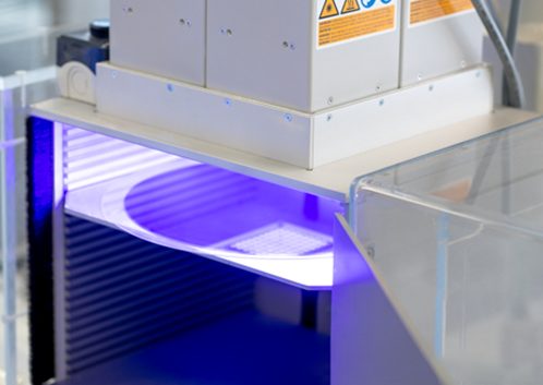
Fan out wafer level packaging (FOWLP) is a cost-effective method in the semiconductor industry. But the typical side effects of this process are warping and chip offset. Despite the continuous improvement of wafer level and panel level fan out technology, these issues related to molding still exist.
Warping is caused by chemical shrinkage of liquid compression molding compound (LCM) during curing and cooling after molding. The second reason for warping is the mismatch in coefficient of thermal expansion (CTE) between the silicon chip, molding material, and substrate. Offset is due to the fact that viscous molding materials with high filler content can usually only be used under high temperature and high pressure. As the chip is fixed to the carrier through temporary bonding, increasing temperature will soften the adhesive, thereby weakening its adhesive strength and reducing its ability to fix the chip. The second reason for the offset is that the pressure required for molding creates stress on each chip.
In order to find solutions to these challenges, DELO conducted a feasibility study by bonding a simple analog chip onto a carrier. In terms of setup, the carrier wafer is coated with temporary bonding adhesive, and the chip is placed face down. Subsequently, the wafer was molded using low viscosity DELO adhesive and cured with ultraviolet radiation before removing the carrier wafer. In such applications, high viscosity thermosetting molding composites are typically used.
DELO also compared the warpage of thermosetting molding materials and UV cured products in the experiment, and the results showed that typical molding materials would warp during the cooling period after thermosetting. Therefore, using room temperature ultraviolet curing instead of heating curing can greatly reduce the impact of thermal expansion coefficient mismatch between the molding compound and the carrier, thereby minimizing warping to the greatest extent possible.
The use of ultraviolet curing materials can also reduce the use of fillers, thereby reducing viscosity and Young’s modulus. The viscosity of the model adhesive used in the test is 35000 mPa · s, and the Young’s modulus is 1 GPa. Due to the absence of heating or high pressure on the molding material, chip offset can be minimized to the greatest extent possible. A typical molding compound has a viscosity of about 800000 mPa · s and a Young’s modulus in the range of two digits.
Overall, research has shown that using UV cured materials for large-area molding is beneficial for producing chip leader fan out wafer level packaging, while minimizing warpage and chip offset to the greatest extent possible. Despite significant differences in thermal expansion coefficients between the materials used, this process still has multiple applications due to the absence of temperature variation. In addition, UV curing can also reduce curing time and energy consumption.
UV instead of thermal curing reduces warpage and die shift in fan-out wafer-level packaging
Comparison of 12-inch coated wafers using a thermally cured, high-filler compound (A) and a UV-cured compound (B)
Post time: Nov-05-2024


