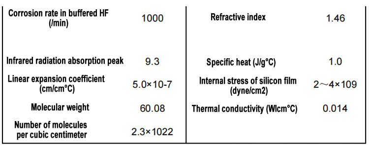
The formation of silicon dioxide on the surface of silicon is called oxidation, and the creation of stable and strongly adherent silicon dioxide led to the birth of silicon integrated circuit planar technology. Although there are many ways to grow silicon dioxide directly on the surface of silicon, it is usually done by thermal oxidation, which is to expose the silicon to a high temperature oxidizing environment (oxygen, water). Thermal oxidation methods can control the film thickness and silicon/silicon dioxide interface characteristics during the preparation of silicon dioxide films. Other techniques for growing silicon dioxide are plasma anodization and wet anodization, but neither of these techniques has been widely used in VLSI processes.
Silicon shows a tendency to form stable silicon dioxide. If freshly cleaved silicon is exposed to an oxidizing environment (such as oxygen, water), it will form a very thin oxide layer (<20Å) even at room temperature. When silicon is exposed to an oxidizing environment at high temperature, a thicker oxide layer will be generated at a faster rate. The basic mechanism of silicon dioxide formation from silicon is well understood. Deal and Grove developed a mathematical model that accurately describes the growth dynamics of oxide films thicker than 300Å. They proposed that oxidation is carried out in the following way, that is, the oxidant (water molecules and oxygen molecules) diffuses through the existing oxide layer to the Si/SiO2 interface, where the oxidant reacts with silicon to form silicon dioxide. The main reaction to form silicon dioxide is described as follows:
The oxidation reaction occurs at the Si/SiO2 interface, so when the oxide layer grows, silicon is continuously consumed and the interface gradually invades silicon. According to the corresponding density and molecular weight of silicon and silicon dioxide, it can be found that the silicon consumed for the thickness of the final oxide layer is 44%. In this way, if the oxide layer grows 10,000Å, 4400Å of silicon will be consumed. This relationship is important for calculating the height of the steps formed on the silicon wafer. The steps are the result of different oxidation rates at different places on the silicon wafer surface.
We also supply high-purity graphite and silicon carbide products, which widely used in wafer processing like oxidation, diffusion, and annealing.
Welcome any customers from all over the world to visit us for a further discussion!
https://www.vet-china.com/
Post time: Nov-13-2024


