Wafer cutting is one of the important links in power semiconductor production. This step is designed to accurately separate individual integrated circuits or chips from semiconductor wafers.
The key to wafer cutting is to be able to separate individual chips while ensuring that the delicate structures and circuits embedded in the wafer are not damaged. The success or failure of the cutting process not only affects the separation quality and yield of the chip, but is also directly related to the efficiency of the entire production process.
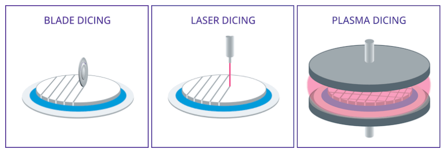
▲Three common types of wafer cutting | Source: KLA CHINA
Currently, the common wafer cutting processes are divided into:
Blade cutting: low cost, usually used for thicker wafers
Laser cutting: high cost, usually used for wafers with a thickness of more than 30μm
Plasma cutting: high cost, more restrictions, usually used for wafers with a thickness of less than 30μm
Mechanical blade cutting
Blade cutting is a process of cutting along the scribe line by a high-speed rotating grinding disk (blade). The blade is usually made of abrasive or ultra-thin diamond material, suitable for slicing or grooving on silicon wafers. However, as a mechanical cutting method, blade cutting relies on physical material removal, which can easily lead to chipping or cracking of the chip edge, thus affecting product quality and reducing yield.
The quality of the final product produced by the mechanical sawing process is affected by multiple parameters, including cutting speed, blade thickness, blade diameter, and blade rotation speed.
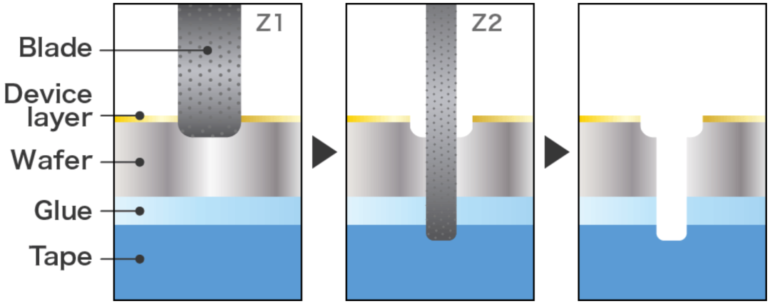
Full cut is the most basic blade cutting method, which completely cuts the workpiece by cutting to a fixed material (such as a slicing tape).
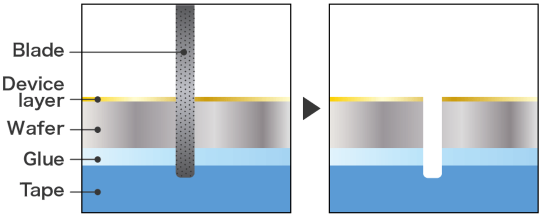
▲ Mechanical blade cutting-full cut | Image source network
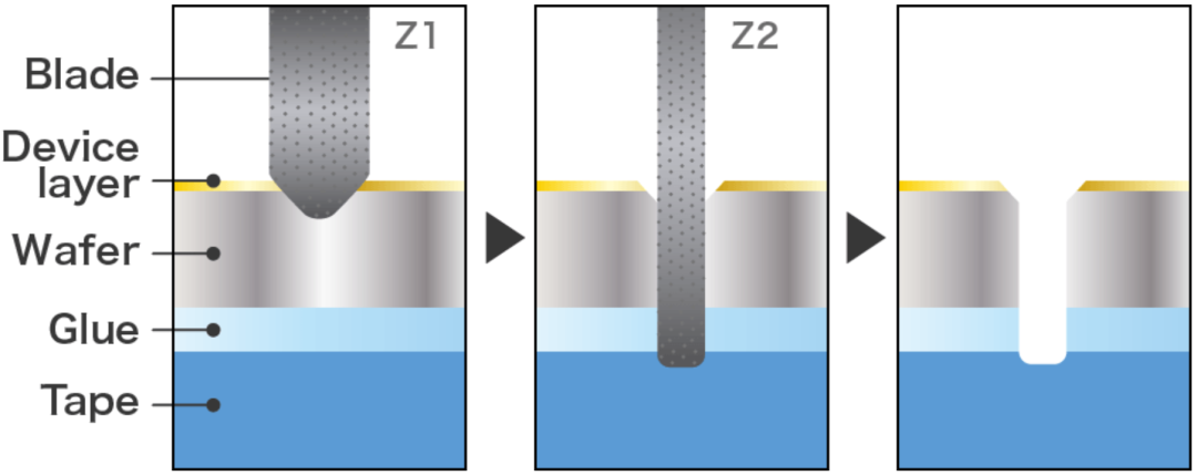
Half cut is a processing method that produces a groove by cutting to the middle of the workpiece. By continuously performing the grooving process, comb and needle-shaped points can be produced.
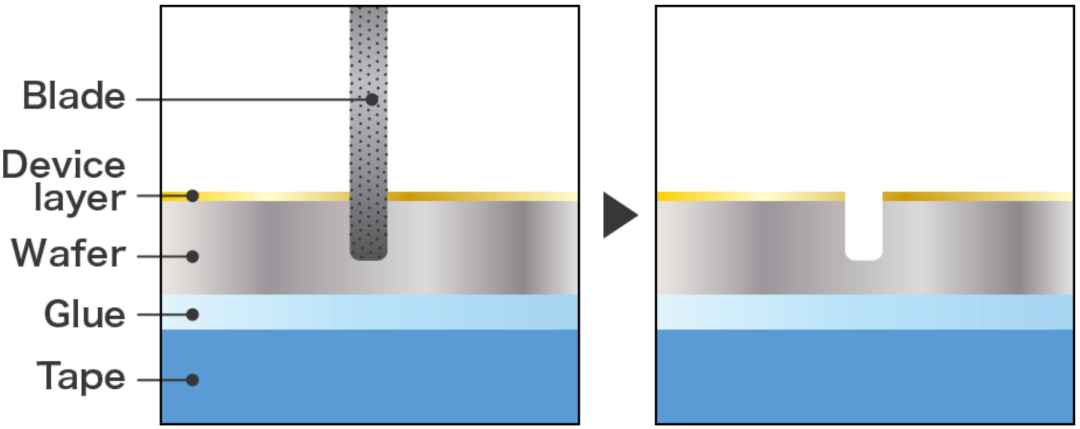
▲ Mechanical blade cutting-half cut | Image source network
Double cut is a processing method that uses a double slicing saw with two spindles to perform full or half cuts on two production lines at the same time. The double slicing saw has two spindle axes. High throughput can be achieved through this process.
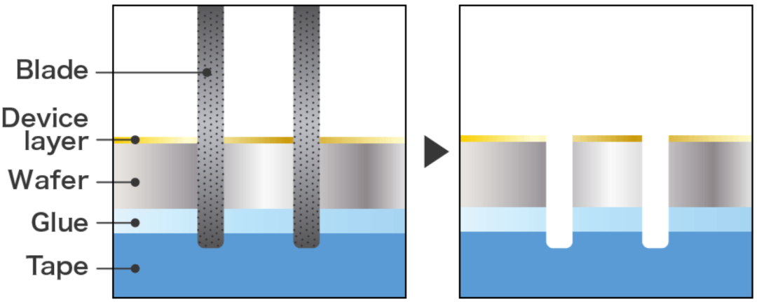
▲ Mechanical blade cutting-double cut | Image source network
Step cut uses a double slicing saw with two spindles to perform full and half cuts in two stages. Use blades optimized for cutting the wiring layer on the surface of the wafer and blades optimized for the remaining silicon single crystal to achieve high-quality processing.
▲ Mechanical blade cutting – step cutting | Image source network
Bevel cutting is a processing method that uses a blade with a V-shaped edge on the half-cut edge to cut the wafer in two stages during the step cutting process. The chamfering process is performed during the cutting process. Therefore, high mold strength and high-quality processing can be achieved.
▲ Mechanical blade cutting – bevel cutting | Image source network
Laser cutting
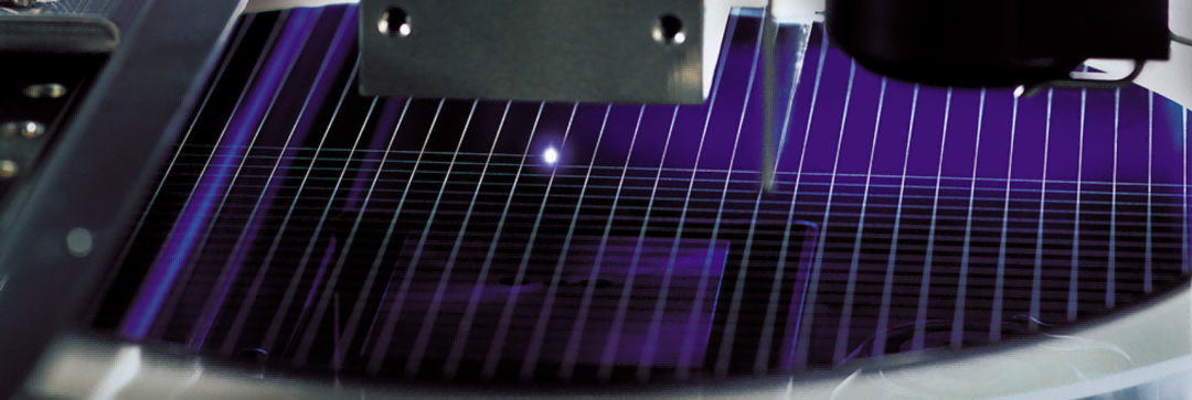
Laser cutting is a non-contact wafer cutting technology that uses a focused laser beam to separate individual chips from semiconductor wafers. The high-energy laser beam is focused on the surface of the wafer and evaporates or removes material along the predetermined cutting line through ablation or thermal decomposition processes.
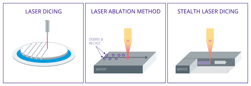
▲ Laser cutting diagram | Image source: KLA CHINA
The types of lasers currently widely used include ultraviolet lasers, infrared lasers, and femtosecond lasers. Among them, ultraviolet lasers are often used for precise cold ablation due to their high photon energy, and the heat-affected zone is extremely small, which can effectively reduce the risk of thermal damage to the wafer and its surrounding chips. Infrared lasers are better suited for thicker wafers because they can penetrate deeply into the material. Femtosecond lasers achieve high-precision and efficient material removal with almost negligible heat transfer through ultrashort light pulses.
Laser cutting has significant advantages over traditional blade cutting. First, as a non-contact process, laser cutting does not require physical pressure on the wafer, reducing the fragmentation and cracking problems common in mechanical cutting. This feature makes laser cutting particularly suitable for processing fragile or ultra-thin wafers, especially those with complex structures or fine features.
▲ Laser cutting diagram | Image source network
In addition, the high precision and accuracy of laser cutting enables it to focus the laser beam to an extremely small spot size, support complex cutting patterns, and achieve separation of the minimum spacing between chips. This feature is particularly important for advanced semiconductor devices with shrinking sizes.
However, laser cutting also has some limitations. Compared with blade cutting, it is slower and more expensive, especially in large-scale production. In addition, choosing the right laser type and optimizing parameters to ensure efficient material removal and minimal heat-affected zone can be challenging for certain materials and thicknesses.
Laser ablation cutting
During laser ablation cutting, the laser beam is precisely focused on a specified location on the surface of the wafer, and the laser energy is guided according to a predetermined cutting pattern, gradually cutting through the wafer to the bottom. Depending on the cutting requirements, this operation is performed using a pulsed laser or a continuous wave laser. In order to prevent damage to the wafer due to excessive local heating of the laser, cooling water is used to cool down and protect the wafer from thermal damage. At the same time, cooling water can also effectively remove particles generated during the cutting process, prevent contamination and ensure cutting quality.
Laser invisible cutting
The laser can also be focused to transfer heat into the main body of the wafer, a method called “invisible laser cutting”. For this method, the heat from the laser creates gaps in the scribe lanes. These weakened areas then achieve a similar penetration effect by breaking when the wafer is stretched.
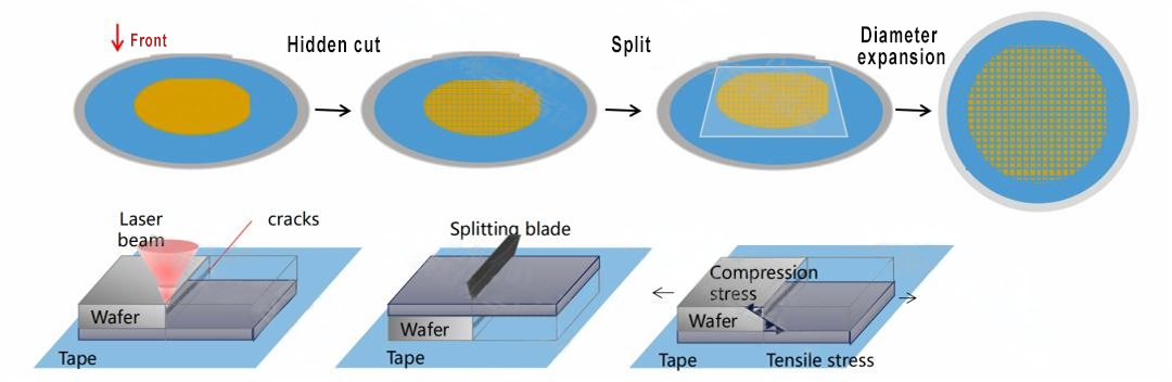
▲Main process of laser invisible cutting
The invisible cutting process is an internal absorption laser process, rather than laser ablation where the laser is absorbed on the surface. With invisible cutting, laser beam energy with a wavelength that is semi-transparent to the wafer substrate material is used. The process is divided into two main steps, one is a laser-based process, and the other is a mechanical separation process.
▲The laser beam creates a perforation below the wafer surface, and the front and back sides are not affected | Image source network
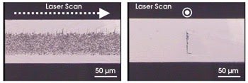
In the first step, as the laser beam scans the wafer, the laser beam focuses on a specific point inside the wafer, forming a cracking point inside. The beam energy causes a series of cracks to form inside, which have not yet extended through the entire thickness of the wafer to the top and bottom surfaces.
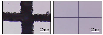
▲Comparison of 100μm thick silicon wafers cut by blade method and laser invisible cutting method | Image source network
In the second step, the chip tape at the bottom of the wafer is physically expanded, which causes tensile stress in the cracks inside the wafer, which are induced in the laser process in the first step. This stress causes the cracks to extend vertically to the upper and lower surfaces of the wafer, and then separate the wafer into chips along these cutting points. In invisible cutting, half-cutting or bottom-side half-cutting is usually used to facilitate the separation of wafers into chips or chips.
Key advantages of invisible laser cutting over laser ablation:
• No coolant required
• No debris generated
• No heat-affected zones that could damage sensitive circuits
Plasma cutting
Plasma cutting (also known as plasma etching or dry etching) is an advanced wafer cutting technology that uses reactive ion etching (RIE) or deep reactive ion etching (DRIE) to separate individual chips from semiconductor wafers. The technology achieves cutting by chemically removing material along predetermined cutting lines using plasma.
During the plasma cutting process, the semiconductor wafer is placed in a vacuum chamber, a controlled reactive gas mixture is introduced into the chamber, and an electric field is applied to generate a plasma containing a high concentration of reactive ions and radicals. These reactive species interact with the wafer material and selectively remove wafer material along the scribe line through a combination of chemical reaction and physical sputtering.
The main advantage of plasma cutting is that it reduces mechanical stress on the wafer and chip and reduces potential damage caused by physical contact. However, this process is more complex and time-consuming than other methods, especially when dealing with thicker wafers or materials with high etching resistance, so its application in mass production is limited.
▲Image source network
In semiconductor manufacturing, the wafer cutting method needs to be selected based on many factors, including wafer material properties, chip size and geometry, required precision and accuracy, and overall production cost and efficiency.
Post time: Sep-20-2024