The manufacturing of each semiconductor product requires hundreds of processes. We divide the entire manufacturing process into eight steps: wafer processing-oxidation-photolithography-etching-thin film deposition-epitaxial growth-diffusion-ion implantation.
To help you understand and recognize semiconductors and related processes, we will push WeChat articles in each issue to introduce each of the above steps one by one.
In the previous article, it was mentioned that in order to protect the wafer from various impurities, an oxide film was made--oxidation process. Today we will discuss the "photolithography process" of photographing the semiconductor design circuit on the wafer with the oxide film formed.
Photolithography process
1. What is photolithography process
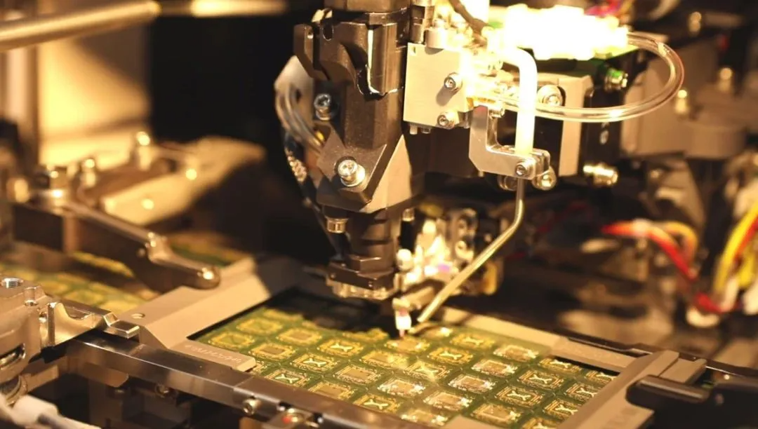
Photolithography is to make the circuits and functional areas required for chip production.
The light emitted by the photolithography machine is used to expose the thin film coated with photoresist through a mask with a pattern. The photoresist will change its properties after seeing the light, so that the pattern on the mask is copied to the thin film, so that the thin film has the function of an electronic circuit diagram. This is the role of photolithography, similar to taking pictures with a camera. The photos taken by the camera are printed on the film, while the photolithography does not engrave photos, but circuit diagrams and other electronic components.
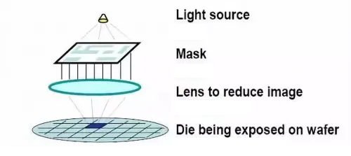
Photolithography is a precise micro-machining technology
Conventional photolithography is a process that uses ultraviolet light with a wavelength of 2000 to 4500 angstroms as the image information carrier, and uses photoresist as the intermediate (image recording) medium to achieve the transformation, transfer and processing of graphics, and finally transmits the image information to the chip (mainly silicon chip) or dielectric layer.
It can be said that photolithography is the foundation of modern semiconductor, microelectronics, and information industries, and photolithography directly determines the development level of these technologies.
In the more than 60 years since the successful invention of integrated circuits in 1959, the line width of its graphics has been reduced by about four orders of magnitude, and the circuit integration has been improved by more than six orders of magnitude. The rapid progress of these technologies is mainly attributed to the development of photolithography.
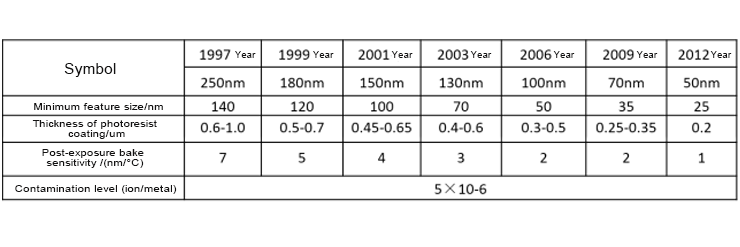
(Requirements for photolithography technology at various stages of development of integrated circuit manufacturing)
2. Basic principles of photolithography
Photolithography materials generally refer to photoresists, also known as photoresists, which are the most critical functional materials in photolithography. This type of material has the characteristics of light (including visible light, ultraviolet light, electron beam, etc.) reaction. After photochemical reaction, its solubility changes significantly.
Among them, the solubility of positive photoresist in the developer increases, and the obtained pattern is the same as the mask; negative photoresist is the opposite, that is, the solubility decreases or even becomes insoluble after being exposed to the developer, and the obtained pattern is opposite to the mask. The application fields of the two types of photoresists are different. Positive photoresists are more commonly used, accounting for more than 80% of the total.
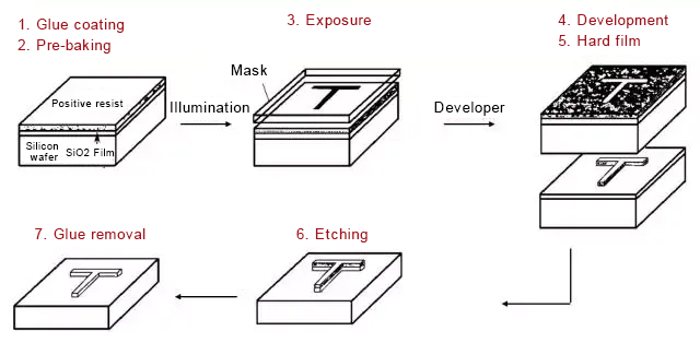 The above is a schematic diagram of the photolithography process
(1) Gluing:
That is, forming a photoresist film with uniform thickness, strong adhesion and no defects on the silicon wafer. In order to enhance the adhesion between the photoresist film and the silicon wafer, it is often necessary to first modify the surface of the silicon wafer with substances such as hexamethyldisilazane (HMDS) and trimethylsilyldiethylamine (TMSDEA). Then, the photoresist film is prepared by spin coating.
(2) Pre-baking:
After spin coating, the photoresist film still contains a certain amount of solvent. After baking at a higher temperature, the solvent can be removed as little as possible. After pre-baking, the content of the photoresist is reduced to about 5%.
(3) Exposure:
That is, the photoresist is exposed to light. At this time, a photoreaction occurs, and the solubility difference between the illuminated part and the non-illuminated part occurs.
(4) Development & hardening:
The product is immersed in the developer. At this time, the exposed area of the positive photoresist and the non-exposed area of the negative photoresist will dissolve in the development. This presents a three-dimensional pattern. After development, the chip needs a high-temperature treatment process to become a hard film, which mainly serves to further enhance the adhesion of the photoresist to the substrate.
(5) Etching:
The material under the photoresist is etched. It includes liquid wet etching and gaseous dry etching. For example, for wet etching of silicon, an acidic aqueous solution of hydrofluoric acid is used; for wet etching of copper, a strong acid solution such as nitric acid and sulfuric acid is used, while dry etching often uses plasma or high-energy ion beams to damage the surface of the material and etch it.
(6) Degumming:
Finally, the photoresist needs to be removed from the surface of the lens. This step is called degumming.
Safety is the most important issue in all semiconductor production. The main dangerous and harmful photolithography gases in the chip lithography process are as follows:
1. Hydrogen peroxide
Hydrogen peroxide (H2O2) is a strong oxidant. Direct contact can cause skin and eye inflammation and burns.
2. Xylene
Xylene is a solvent and developer used in negative lithography. It is flammable and has a low temperature of only 27.3℃ (approximately room temperature). It is explosive when the concentration in the air is 1%-7%. Repeated contact with xylene can cause skin inflammation. Xylene vapor is sweet, similar to the smell of airplane tack; exposure to xylene can cause inflammation of the eyes, nose and throat. Inhalation of the gas can cause headaches, dizziness, loss of appetite and fatigue.
3. Hexamethyldisilazane (HMDS)
Hexamethyldisilazane (HMDS) is most commonly used as a primer layer to increase the adhesion of photoresist on the surface of the product. It is flammable and has a flash point of 6.7°C. It is explosive when the concentration in the air is 0.8%-16%. HMDS reacts strongly with water, alcohol and mineral acids to release ammonia.
4. Tetramethylammonium hydroxide
Tetramethylammonium hydroxide (TMAH) is widely used as a developer for positive lithography. It is toxic and corrosive. It can be fatal if swallowed or in direct contact with the skin. Contact with TMAH dust or mist can cause inflammation of the eyes, skin, nose and throat. Inhalation of high concentrations of TMAH will lead to death.
5. Chlorine and fluorine
Chlorine (Cl2) and fluorine (F2) are both used in excimer lasers as deep ultraviolet and extreme ultraviolet (EUV) light sources. Both gases are toxic, appear light green, and have a strong irritating odor. Inhalation of high concentrations of this gas will lead to death. Fluorine gas may react with water to produce hydrogen fluoride gas. Hydrogen fluoride gas is a strong acid that irritates the skin, eyes and respiratory tract and may cause symptoms such as burns and difficulty breathing. High Concentrations of fluoride can cause poisoning to the human body, causing symptoms such as headaches, vomiting, diarrhea, and coma.
6. Argon
Argon (Ar) is an inert gas that usually does not cause direct harm to the human body. Under normal circumstances, the air people breathe contains about 0.93% argon, and this concentration has no obvious effect on the human body. However, in some cases, argon may cause harm to the human body.
Here are some possible situations: In a confined space, the concentration of argon may increase, thereby reducing the oxygen concentration in the air and causing hypoxia. This may cause symptoms such as dizziness, fatigue, and shortness of breath. In addition, argon is an inert gas, but it may explode under high temperature or high pressure.
7. Neon
Neon (Ne) is a stable, colorless and odorless gas that does not participate in The neon gas is not involved in the human respiratory process, so breathing in a high concentration of neon gas will cause hypoxia. If you are in a state of hypoxia for a long time, you may experience symptoms such as headache, nausea, and vomiting. In addition, neon gas may react with other substances under high temperature or high pressure to cause fire or explosion.
8. Xenon gas
Xenon gas (Xe) is a stable, colorless and odorless gas that does not participate in the human respiratory process, so breathing in a high concentration of xenon gas will cause hypoxia. If you are in a state of hypoxia for a long time, you may experience symptoms such as headache, nausea, and vomiting. In addition, neon gas may react with other substances under high temperature or high pressure to cause fire or explosion.
9. Krypton gas
Krypton gas (Kr) is a stable, colorless and odorless gas that does not participate in the human respiratory process, so breathing in a high concentration of krypton gas will cause hypoxia. If you are in a state of hypoxia for a long time, you may experience symptoms such as headache, nausea, and vomiting. In addition, xenon gas may react with other substances under high temperature or high pressure to cause fire or explosion. Breathing in an environment with oxygen deprivation can cause hypoxia. If you are in a state of hypoxia for a long time, you may experience symptoms such as headache, nausea, and vomiting. In addition, krypton gas may react with other substances under high temperature or high pressure to cause fire or explosion.
Hazardous gas detection solutions for the semiconductor industry
The semiconductor industry involves the production, manufacturing, and process of flammable, explosive, toxic, and harmful gases. As a user of gases in semiconductor manufacturing plants, every staff member should understand the safety data of various hazardous gases before use, and should know how to deal with the emergency procedures when these gases leak.
In the production, manufacturing, and storage of the semiconductor industry, in order to avoid the loss of life and property caused by the leakage of these hazardous gases, it is necessary to install gas detection instruments to detect the target gas.
Gas detectors have become essential environmental monitoring instruments in today's semiconductor industry, and are also the most direct monitoring tools.
Riken Keiki has always paid attention to the safe development of the semiconductor manufacturing industry, with the mission of creating a safe working environment for people, and has devoted itself to developing gas sensors suitable for the semiconductor industry, providing reasonable solutions for various problems encountered by users, and continuously upgrading product functions and optimizing systems.
Post time: Jul-16-2024