Welcome to our website for product information and consultation.
Our website: https://www.vet-china.com/
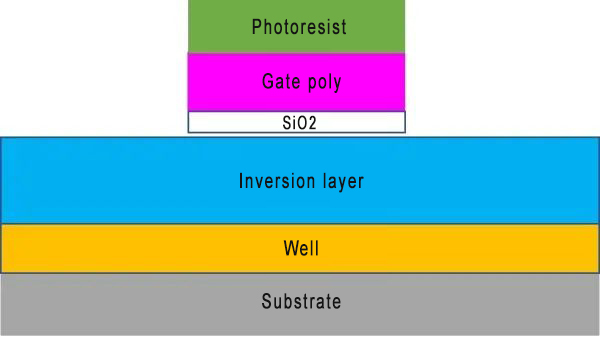
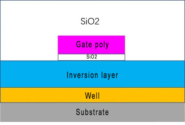
Etching of Poly and SiO2:
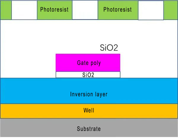
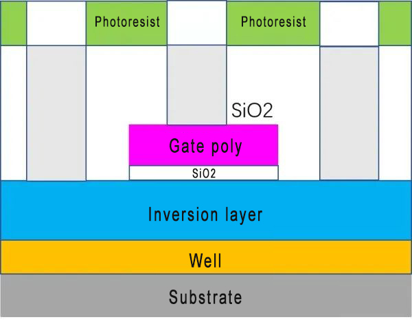
After this, the excess Poly and SiO2 are etched away, that is, removed. At this time, directional etching is used. In the classification of etching, there is a classification of directional etching and non-directional etching. Directional etching refers to etching in a certain direction, while non-directional etching is non-directional (I accidentally said too much. In short, it is to remove SiO2 in a certain direction through specific acids and bases). In this example, we use downward directional etching to remove SiO2, and it becomes like this.
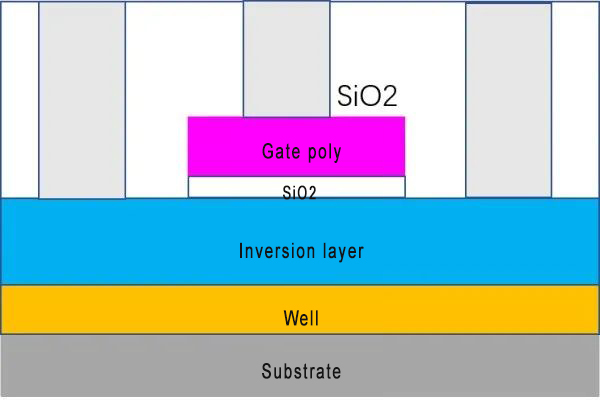
Finally, remove the photoresist. At this time, the method of removing the photoresist is not the activation through light irradiation mentioned above, but through other methods, because we do not need to define a specific size at this time, but to remove all the photoresist. Finally, it becomes as shown in the following figure.
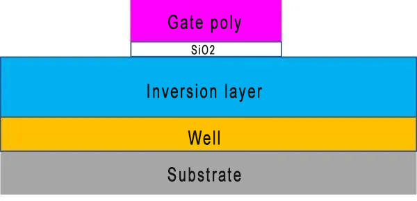
In this way, we have achieved the purpose of retaining the specific location of the Poly SiO2.
Formation of the source and drain:
Finally, let's consider how the source and drain are formed. Everyone still remembers that we talked about it in the last issue. The source and drain are ion-implanted with the same type of elements. At this time, we can use photoresist to open the source/drain area where the N type needs to be implanted. Since we only take NMOS as an example, all parts in the above figure will be opened, as shown in the following figure.
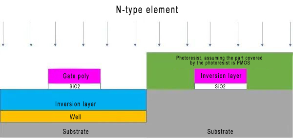
Since the part covered by the photoresist cannot be implanted (the light is blocked), N-type elements will only be implanted on the required NMOS. Since the substrate under the poly is blocked by poly and SiO2, it will not be implanted, so it becomes like this.
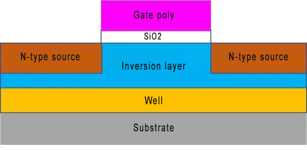
At this point, a simple MOS model has been made. In theory, if voltage is added to the source, drain, poly and substrate, this MOS can work, but we can't just take a probe and add voltage directly to the source and drain. At this time, MOS wiring is needed, that is, on this MOS, connect wires to connect many MOS together. Let's take a look at the wiring process.
Making VIA:
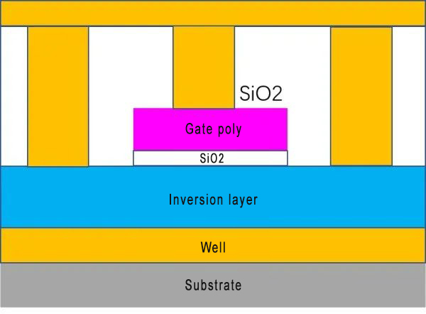
The first step is to cover the entire MOS with a layer of SiO2, as shown in the figure below:
Of course, this SiO2 is produced by CVD, because it is very fast and saves time. The following is still the process of laying photoresist and exposing. After the end, it looks like this.
Then use the etching method to etch a hole on the SiO2, as shown in the gray part in the figure below. The depth of this hole directly contacts the Si surface.
Finally, remove the photoresist and get the following appearance.
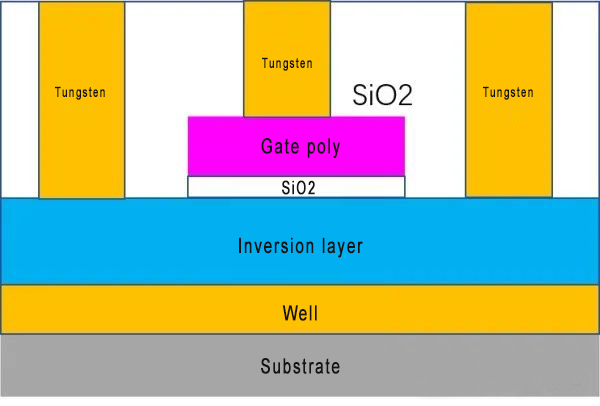
At this time, what needs to be done is to fill the conductor in this hole. As for what this conductor is? Each company is different, most of them are tungsten alloys, so how can this hole be filled? The PVD (Physical Vapor Deposition) method is used, and the principle is similar to the figure below.
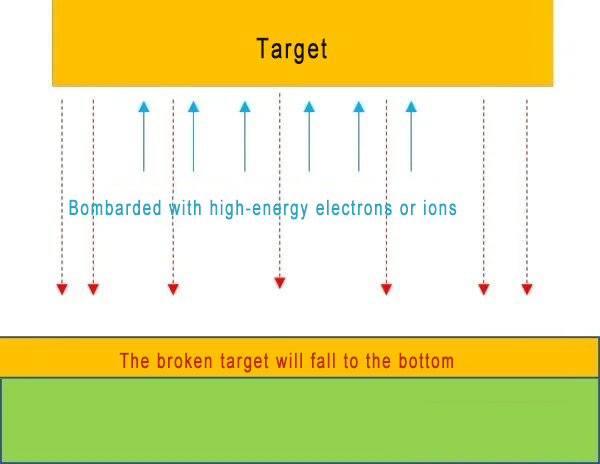
Use high-energy electrons or ions to bombard the target material, and the broken target material will fall to the bottom in the form of atoms, thus forming the coating below. The target material we usually see in the news refers to the target material here.
After filling the hole, it looks like this.
Of course, when we fill it, it is impossible to control the thickness of the coating to be exactly equal to the depth of the hole, so there will be some excess, so we use CMP (Chemical Mechanical Polishing) technology, which sounds very high-end, but it is actually grinding, grinding away the excess parts. The result is like this.
At this point, we have completed the production of a layer of via. Of course, the production of via is mainly for the wiring of the metal layer behind.
Metal layer production:
Under the above conditions, we use PVD to dep another layer of metal. This metal is mainly a copper-based alloy.
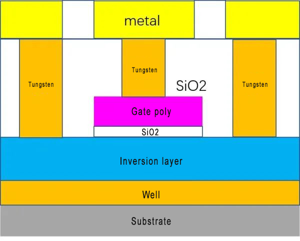
Then after exposure and etching, we get what we want. Then continue to stack up until we meet our needs.

When we draw the layout, we will tell you how many layers of metal and via the process used can be stacked at most, which means how many layers it can be stacked.
Finally, we get this structure. The top pad is the pin of this chip, and after packaging, it becomes the pin we can see (of course, I drew it randomly, there is no practical significance, just for example).
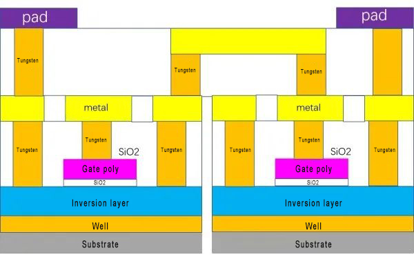
This is the general process of making a chip. In this issue, we learned about the most important exposure, etching, ion implantation, furnace tubes, CVD, PVD, CMP, etc. in semiconductor foundry.
Post time: Aug-23-2024