You can understand it even if you have never studied physics or mathematics, but it is a bit too simple and suitable for beginners. If you want to know more about CMOS, you have to read the content of this issue, because only after understanding the process flow (that is, the production process of the diode) can you continue to understand the following content. Then let's learn about how this CMOS is produced in the foundry company in this issue (taking non-advanced process as an example, the CMOS of advanced process is different in structure and production principle).
First of all, you must know that the wafers that the foundry gets from the supplier (silicon wafer supplier) are one by one, with a radius of 200mm (8-inch factory) or 300mm (12-inch factory). As shown in the figure below, it is actually similar to a big cake, which we call a substrate.
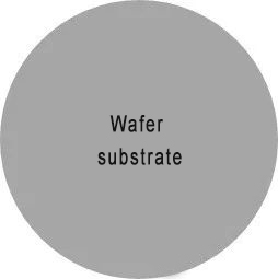
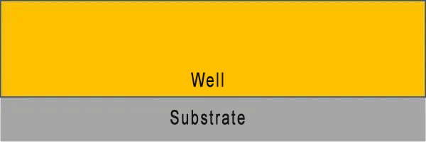
However, it is not convenient for us to look at it this way. We look from the bottom up and look at the cross-sectional view, which becomes the following figure.

Next, let's see how the CMOS model appears. Since the actual process requires thousands of steps, I will talk about the main steps of the simplest 8-inch wafer here.
Making Well and Inversion Layer:
That is, the well is implanted into the substrate by ion implantation (Ion Implantation, hereinafter referred to as imp). If you want to make NMOS, you need to implant P-type wells. If you want to make PMOS, you need to implant N-type wells. For your convenience, let's take NMOS as an example. The ion implantation machine implants the P-type elements to be implanted into the substrate to a specific depth, and then heats them at high temperature in the furnace tube to activate these ions and diffuse them around. This completes the production of the well. This is what it looks like after the production is completed.
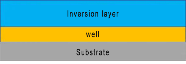
After making the well, there are other ion implantation steps, the purpose of which is to control the size of the channel current and threshold voltage. Everyone can call it the inversion layer. If you want to make NMOS, the inversion layer is implanted with P-type ions, and if you want to make PMOS, the inversion layer is implanted with N-type ions. After implantation, it is the following model.
There are a lot of contents here, such as the energy, angle, ion concentration during ion implantation, etc., which are not included in this issue, and I believe that if you know those things, you must be an insider, and you must have a way to learn them.
Making SiO2:
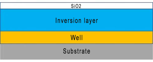
Silicon dioxide (SiO2, hereinafter referred to as oxide) will be made later. In the CMOS production process, there are many ways to make oxide. Here, SiO2 is used under the gate, and its thickness directly affects the size of the threshold voltage and the size of the channel current. Therefore, most foundries choose the furnace tube oxidation method with the highest quality, the most precise thickness control, and the best uniformity at this step. In fact, it is very simple, that is, in a furnace tube with oxygen, high temperature is used to allow oxygen and silicon to react chemically to generate SiO2. In this way, a thin layer of SiO2 is generated on the surface of Si, as shown in the figure below.
Of course, there is also a lot of specific information here, such as how many degrees are needed, how much concentration of oxygen is needed, how long the high temperature is needed, etc. These are not what we are considering now, those are too specific.
Formation of gate end Poly:
But it is not over yet. SiO2 is just equivalent to a thread, and the real gate (Poly) has not started yet. So our next step is to lay a layer of polysilicon on SiO2 (polysilicon is also composed of a single silicon element, but the lattice arrangement is different. Don't ask me why the substrate uses single crystal silicon and the gate uses polysilicon. There is a book called Semiconductor Physics. You can learn about it. It's embarrassing~). Poly is also a very critical link in CMOS, but the component of poly is Si, and it cannot be generated by direct reaction with Si substrate like growing SiO2. This requires the legendary CVD (Chemical Vapor Deposition), which is to react chemically in a vacuum and precipitate the generated object on the wafer. In this example, the generated substance is polysilicon, and then precipitated on the wafer (here I have to say that poly is generated in a furnace tube by CVD, so the generation of poly is not done by a pure CVD machine).
But the polysilicon formed by this method will be precipitated on the entire wafer, and it looks like this after precipitation.

Exposure of Poly and SiO2:
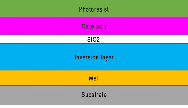
At this step, the vertical structure we want has actually been formed, with poly on the top, SiO2 on the bottom, and the substrate on the bottom. But now the whole wafer is like this, and we only need a specific position to be the "faucet" structure. So there is the most critical step in the entire process - exposure.
We first spread a layer of photoresist on the surface of the wafer, and it becomes like this.
Then put the defined mask (the circuit pattern has been defined on the mask) on it, and finally irradiate it with light of a specific wavelength. The photoresist will become activated in the irradiated area. Since the area blocked by the mask is not illuminated by the light source, this piece of photoresist is not activated.
Since the activated photoresist is particularly easy to be washed away by a specific chemical liquid, while the unactivated photoresist cannot be washed away, after irradiation, a specific liquid is used to wash away the activated photoresist, and finally it becomes like this, leaving the photoresist where Poly and SiO2 need to be retained, and removing the photoresist where it does not need to be retained.
Post time: Aug-23-2024