Early wet etching promoted the development of cleaning or ashing processes. Today, dry etching using plasma has become the mainstream etching process. Plasma consists of electrons, cations and radicals. The energy applied to the plasma causes the outermost electrons of the source gas in a neutral state to be stripped off, thereby converting these electrons into cations.
In addition, imperfect atoms in molecules can be stripped off by applying energy to form electrically neutral radicals. Dry etching uses cations and radicals that make up plasma, where cations are anisotropic (suitable for etching in a certain direction) and radicals are isotropic (suitable for etching in all directions). The number of radicals is far greater than the number of cations. In this case, dry etching should be isotropic like wet etching.
However, it is the anisotropic etching of dry etching that makes ultra-miniaturized circuits possible. What is the reason for this? In addition, the etching speed of cations and radicals is very slow. So how can we apply plasma etching methods to mass production in the face of this shortcoming?
1. Aspect Ratio (A/R)
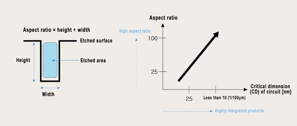
Figure 1. The concept of aspect ratio and the impact of technological progress on it
Aspect Ratio is the ratio of horizontal width to vertical height (i.e., height divided by width). The smaller the critical dimension (CD) of the circuit, the larger the aspect ratio value. That is, assuming an aspect ratio value of 10 and a width of 10nm, the height of the hole drilled during the etching process should be 100nm. Therefore, for next-generation products that require ultra-miniaturization (2D) or high density (3D), extremely high aspect ratio values are required to ensure that cations can penetrate the bottom film during etching.
To achieve ultra-miniaturization technology with a critical dimension of less than 10nm in 2D products, the capacitor aspect ratio value of dynamic random access memory (DRAM) should be maintained above 100. Similarly, 3D NAND flash memory also requires higher aspect ratio values to stack 256 layers or more of cell stacking layers. Even if the conditions required for other processes are met, the required products cannot be produced if the etching process is not up to standard. This is why etching technology is becoming increasingly important.
2. Overview of plasma etching
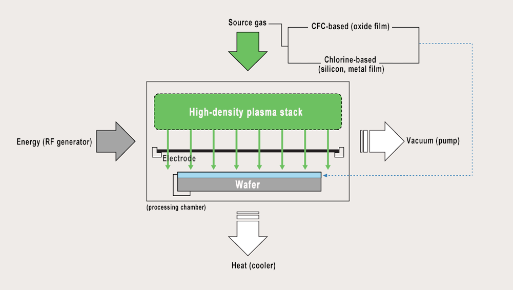
Figure 2. Determining plasma source gas according to film type
When a hollow pipe is used, the narrower the pipe diameter, the easier it is for liquid to enter, which is the so-called capillary phenomenon. However, if a hole (closed end) is to be drilled in the exposed area, the input of the liquid becomes quite difficult. Therefore, since the critical size of the circuit was 3um to 5um in the mid-1970s, dry etching has gradually replaced wet etching as the mainstream. That is, although ionized, it is easier to penetrate deep holes because the volume of a single molecule is smaller than that of an organic polymer solution molecule.
During plasma etching, the interior of the processing chamber used for etching should be adjusted to a vacuum state before injecting the plasma source gas suitable for the relevant layer. When etching solid oxide films, stronger carbon fluoride-based source gases should be used. For relatively weak silicon or metal films, chlorine-based plasma source gases should be used.
So, how should the gate layer and the underlying silicon dioxide (SiO2) insulating layer be etched?
First, for the gate layer, silicon should be removed using a chlorine-based plasma (silicon + chlorine) with polysilicon etching selectivity. For the bottom insulating layer, the silicon dioxide film should be etched in two steps using a carbon fluoride-based plasma source gas (silicon dioxide + carbon tetrafluoride) with stronger etching selectivity and effectiveness.
3. Reactive ion etching (RIE or physicochemical etching) process
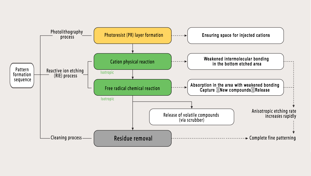
Figure 3. Advantages of reactive ion etching (anisotropy and high etching rate)
Plasma contains both isotropic free radicals and anisotropic cations, so how does it perform anisotropic etching?
Plasma dry etching is mainly performed by reactive ion etching (RIE, Reactive Ion Etching) or applications based on this method. The core of the RIE method is to weaken the binding force between target molecules in the film by attacking the etching area with anisotropic cations. The weakened area is absorbed by free radicals, combined with the particles that make up the layer, converted into gas (a volatile compound) and released.
Although free radicals have isotropic characteristics, molecules that make up the bottom surface (whose binding force is weakened by the attack of cations) are more easily captured by free radicals and converted into new compounds than side walls with strong binding force. Therefore, downward etching becomes the mainstream. The captured particles become gas with free radicals, which are desorbed and released from the surface under the action of vacuum.
At this time, the cations obtained by physical action and the free radicals obtained by chemical action are combined for physical and chemical etching, and the etching rate (Etch Rate, the degree of etching in a certain period of time) is increased by 10 times compared with the case of cationic etching or free radical etching alone. This method can not only increase the etching rate of anisotropic downward etching, but also solve the problem of polymer residue after etching. This method is called reactive ion etching (RIE). The key to the success of RIE etching is to find a plasma source gas suitable for etching the film. Note: Plasma etching is RIE etching, and the two can be regarded as the same concept.
4. Etch Rate and Core Performance Index
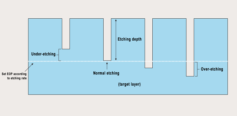
Figure 4. Core Etch Performance Index related to Etch Rate
Etch rate refers to the depth of film that is expected to be reached in one minute. So what does it mean that the etch rate varies from part to part on a single wafer?
This means that the etch depth varies from part to part on the wafer. For this reason, it is very important to set the end point (EOP) where etching should stop by considering the average etch rate and etch depth. Even if the EOP is set, there are still some areas where the etch depth is deeper (over-etched) or shallower (under-etched) than originally planned. However, under-etching causes more damage than over-etching during etching. Because in the case of under-etching, the under-etched part will hinder subsequent processes such as ion implantation.
Meanwhile, selectivity (measured by etch rate) is a key performance indicator of the etching process. The measurement standard is based on the comparison of the etch rate of the mask layer (photoresist film, oxide film, silicon nitride film, etc.) and the target layer. This means that the higher the selectivity, the faster the target layer is etched. The higher the level of miniaturization, the higher the selectivity requirement is to ensure that fine patterns can be perfectly presented. Since the etching direction is straight, the selectivity of cationic etching is low, while the selectivity of radical etching is high, which improves the selectivity of RIE.
5. Etching process
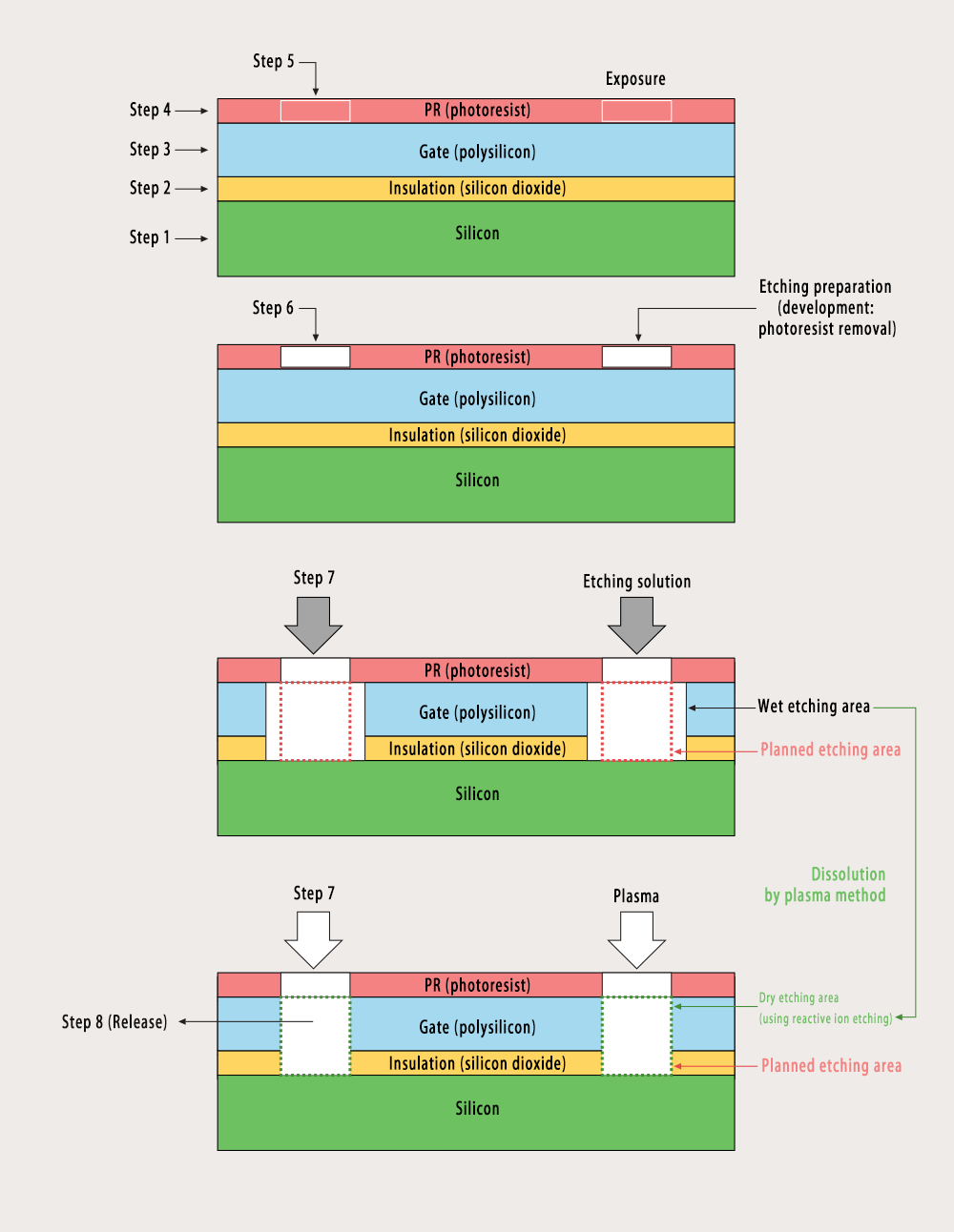
Figure 5. Etching process
First, the wafer is placed in an oxidation furnace with a temperature maintained between 800 and 1000℃, and then a silicon dioxide (SiO2) film with high insulation properties is formed on the surface of the wafer by a dry method. Next, the deposition process is entered to form a silicon layer or a conductive layer on the oxide film by chemical vapor deposition (CVD)/physical vapor deposition (PVD). If a silicon layer is formed, an impurity diffusion process can be performed to increase conductivity if necessary. During the impurity diffusion process, multiple impurities are often added repeatedly.
At this time, the insulating layer and the polysilicon layer should be combined for etching. First, a photoresist is used. Subsequently, a mask is placed on the photoresist film and wet exposure is performed by immersion to imprint the desired pattern (invisible to the naked eye) on the photoresist film. When the pattern outline is revealed by development, the photoresist in the photosensitive area is removed. Then, the wafer processed by the photolithography process is transferred to the etching process for dry etching.
Dry etching is mainly carried out by reactive ion etching (RIE), in which etching is repeated mainly by replacing the source gas suitable for each film. Both dry etching and wet etching aim to increase the aspect ratio (A/R value) of etching. In addition, regular cleaning is required to remove the polymer accumulated at the bottom of the hole (the gap formed by etching). The important point is that all variables (such as materials, source gas, time, form and sequence) should be adjusted organically to ensure that the cleaning solution or plasma source gas can flow down to the bottom of the trench. A slight change in a variable requires recalculation of other variables, and this recalculation process is repeated until it meets the purpose of each stage. Recently, monoatomic layers such as atomic layer deposition (ALD) layers have become thinner and harder. Therefore, etching technology is moving towards the use of low temperatures and pressures. The etching process aims to control the critical dimension (CD) to produce fine patterns and ensure that problems caused by the etching process are avoided, especially under-etching and problems related to residue removal. The above two articles on etching aim to provide readers with an understanding of the purpose of the etching process, the obstacles to achieving the above goals, and the performance indicators used to overcome such obstacles.
Post time: Sep-10-2024