2 Experimental results and discussion
2.1 Epitaxial layer thickness and uniformity
Epitaxial layer thickness, doping concentration and uniformity are one of the core indicators for judging the quality of epitaxial wafers. Accurately controllable thickness, doping concentration and uniformity within the wafer are the key to ensuring the performance and consistency of SiC power devices, and epitaxial layer thickness and doping concentration uniformity are also important bases for measuring the process capability of epitaxial equipment.
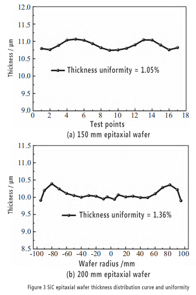
Figure 3 shows the thickness uniformity and distribution curve of 150 mm and 200 mm SiC epitaxial wafers. It can be seen from the figure that the epitaxial layer thickness distribution curve is symmetrical about the center point of the wafer. The epitaxial process time is 600s, the average epitaxial layer thickness of the 150mm epitaxial wafer is 10.89 um, and the thickness uniformity is 1.05%. By calculation, the epitaxial growth rate is 65.3 um/h, which is a typical fast epitaxial process level. Under the same epitaxial process time, the epitaxial layer thickness of the 200 mm epitaxial wafer is 10.10 um, the thickness uniformity is within 1.36%, and the overall growth rate is 60.60 um/h, which is slightly lower than the 150 mm epitaxial growth rate. This is because there is obvious loss along the way when the silicon source and carbon source flow from the upstream of the reaction chamber through the wafer surface to the downstream of the reaction chamber, and the 200 mm wafer area is larger than the 150 mm. The gas flows through the surface of the 200 mm wafer for a longer distance, and the source gas consumed along the way is more. Under the condition that the wafer keeps rotating, the overall thickness of the epitaxial layer is thinner, so the growth rate is slower. Overall, the thickness uniformity of 150 mm and 200 mm epitaxial wafers is excellent, and the process capability of the equipment can meet the requirements of high-quality devices.
2.2 Epitaxial layer doping concentration and uniformity
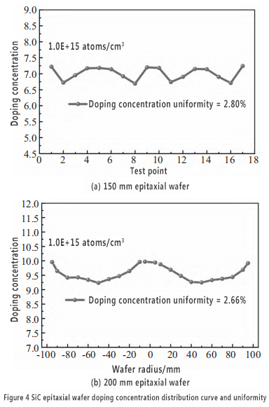
Figure 4 shows the doping concentration uniformity and curve distribution of 150 mm and 200 mm SiC epitaxial wafers. As can be seen from the figure, the concentration distribution curve on the epitaxial wafer has obvious symmetry relative to the center of the wafer. The doping concentration uniformity of the 150 mm and 200 mm epitaxial layers is 2.80% and 2.66% respectively, which can be controlled within 3%, which is an excellent level for similar international equipment. The doping concentration curve of the epitaxial layer is distributed in a "W" shape along the diameter direction, which is mainly determined by the flow field of the horizontal hot wall epitaxial furnace, because the airflow direction of the horizontal airflow epitaxial growth furnace is from the air inlet end (upstream) and flows out from the downstream end in a laminar manner through the wafer surface; because the "along-the-way depletion" rate of the carbon source (C2H4) is higher than that of the silicon source (TCS), when the wafer rotates, the actual C/Si on the wafer surface gradually decreases from the edge to the center (the carbon source in the center is less), according to the "competitive position theory" of C and N, the doping concentration in the center of the wafer gradually decreases toward the edge, in order to obtain excellent concentration uniformity, the edge N2 is added as compensation during the epitaxial process to slow down the decrease in doping concentration from the center to the edge, so that the final doping concentration curve presents a "W" shape.
2.3 Epitaxial layer defects
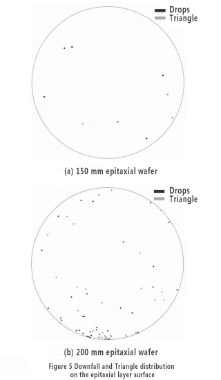
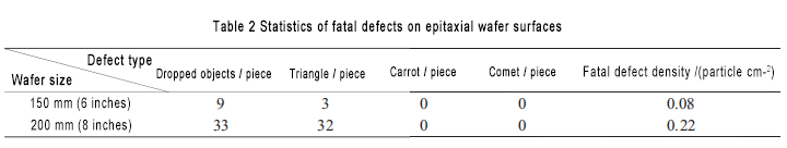
In addition to thickness and doping concentration, the level of epitaxial layer defect control is also a core parameter for measuring the quality of epitaxial wafers and an important indicator of the process capability of epitaxial equipment. Although SBD and MOSFET have different requirements for defects, the more obvious surface morphology defects such as drop defects, triangle defects, carrot defects, comet defects, etc. are defined as killer defects of SBD and MOSFET devices. The probability of failure of chips containing these defects is high, so controlling the number of killer defects is extremely important for improving chip yield and reducing costs. Figure 5 shows the distribution of killer defects of 150 mm and 200 mm SiC epitaxial wafers. Under the condition that there is no obvious imbalance in the C/Si ratio, carrot defects and comet defects can be basically eliminated, while drop defects and triangle defects are related to the cleanliness control during the operation of epitaxial equipment, the impurity level of graphite parts in the reaction chamber, and the quality of the substrate. From Table 2, it can be seen that the killer defect density of 150 mm and 200 mm epitaxial wafers can be controlled within 0.3 particles/cm2, which is an excellent level for the same type of equipment. The fatal defect density control level of 150 mm epitaxial wafer is better than that of 200 mm epitaxial wafer. This is because the substrate preparation process of 150 mm is more mature than that of 200 mm, the substrate quality is better, and the impurity control level of 150 mm graphite reaction chamber is better.
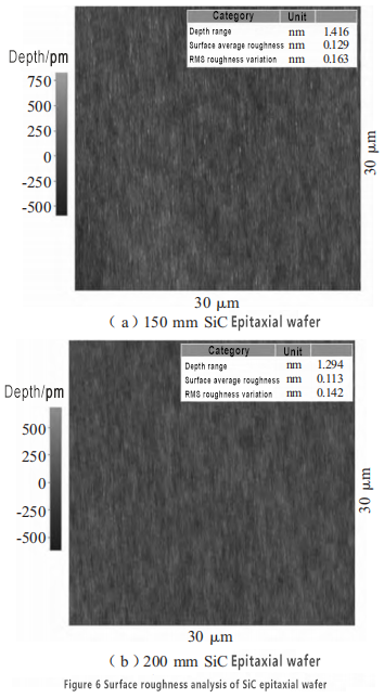
2.4 Epitaxial wafer surface roughness
Figure 6 shows the AFM images of the surface of 150 mm and 200 mm SiC epitaxial wafers. It can be seen from the figure that the surface root mean square roughness Ra of 150 mm and 200 mm epitaxial wafers is 0.129 nm and 0.113 nm respectively, and the surface of the epitaxial layer is smooth without obvious macro-step aggregation phenomenon. This phenomenon shows that the growth of the epitaxial layer always maintains the step flow growth mode during the entire epitaxial process, and no step aggregation occurs. It can be seen that by using the optimized epitaxial growth process, smooth epitaxial layers can be obtained on 150 mm and 200 mm low-angle substrates.
3 Conclusion
The 150 mm and 200 mm 4H-SiC homogeneous epitaxial wafers were successfully prepared on domestic substrates using the self-developed 200 mm SiC epitaxial growth equipment, and the homogeneous epitaxial process suitable for 150 mm and 200 mm was developed. The epitaxial growth rate can be greater than 60 μm/h. While meeting the high-speed epitaxy requirement, the epitaxial wafer quality is excellent. The thickness uniformity of the 150 mm and 200 mm SiC epitaxial wafers can be controlled within 1.5%, the concentration uniformity is less than 3%, the fatal defect density is less than 0.3 particles/cm2, and the epitaxial surface roughness root mean square Ra is less than 0.15 nm. The core process indicators of the epitaxial wafers are at the advanced level in the industry.
Source: Electronic Industry Special Equipment
Author: Xie Tianle, Li Ping, Yang Yu, Gong Xiaoliang, Ba Sai, Chen Guoqin, Wan Shengqiang
(48th Research Institute of China Electronics Technology Group Corporation, Changsha, Hunan 410111)
Post time: Sep-04-2024