2. Epitaxial thin film growth
The substrate provides a physical support layer or conductive layer for Ga2O3 power devices. The next important layer is the channel layer or epitaxial layer used for voltage resistance and carrier transport. In order to increase breakdown voltage and minimize conduction resistance, controllable thickness and doping concentration, as well as optimal material quality, are some prerequisites. High quality Ga2O3 epitaxial layers are typically deposited using molecular beam epitaxy (MBE), metal organic chemical vapor deposition (MOCVD), halide vapor deposition (HVPE), pulsed laser deposition (PLD), and fog CVD based deposition techniques.
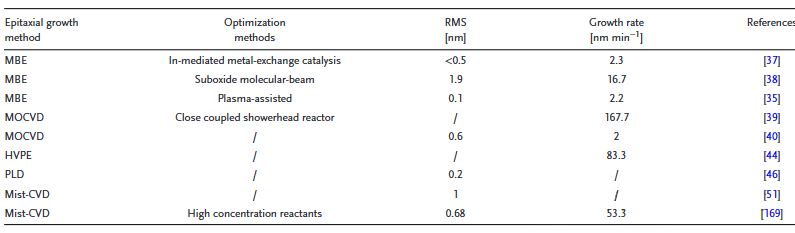
Table 2 Some representative epitaxial technologies
2.1 MBE method
MBE technology is renowned for its ability to grow high-quality, defect-free β-Ga2O3 films with controllable n-type doping due to its ultra-high vacuum environment and high material purity. As a result, it has become one of the most widely studied and potentially commercialized β-Ga2O3 thin film deposition technologies. In addition, the MBE method also successfully prepared a high-quality, low-doped heterostructure β-(AlXGa1-X)2O3/Ga2O3 thin film layer. MBE can monitor surface structure and morphology in real time with atomic layer precision by using reflection high energy electron diffraction (RHEED). However, β-Ga2O3 films grown using MBE technology still face many challenges, such as low growth rate and small film size. The study found that the growth rate was in the order of (010)>(001)>(−201)>(100). Under slightly Ga-rich conditions of 650 to 750°C, β-Ga2O3 (010) exhibits optimal growth with a smooth surface and high growth rate. Using this method, β-Ga2O3 epitaxy was successfully achieved with an RMS roughness of 0.1 nm. β-Ga2O3 In a Ga-rich environment, MBE films grown at different temperatures are shown in the figure. Novel Crystal Technology Inc. has successfully epitaxially produced 10 × 15mm2 β-Ga2O3MBE wafers. They provide high quality (010) oriented β-Ga2O3 single crystal substrates with a thickness of 500 μm and XRD FWHM below 150 arc seconds. The substrate is Sn doped or Fe doped. The Sn-doped conductive substrate has a doping concentration of 1E18 to 9E18cm−3, while the iron-doped semi-insulating substrate has a resistivity higher than 10E10 Ω cm.
2.2 MOCVD method
MOCVD uses metal organic compounds as precursor materials to grow thin films, thereby achieving large-scale commercial production. When growing Ga2O3 using the MOCVD method, trimethylgallium (TMGa), triethylgallium (TEGa) and Ga (dipentyl glycol formate) are usually used as the Ga source, while H2O, O2 or N2O are used as the oxygen source. Growth using this method generally requires high temperatures (>800°C). This technology has the potential to achieve low carrier concentration and high and low temperature electron mobility, so it is of great significance to the realization of high-performance β-Ga2O3 power devices. Compared with the MBE growth method, MOCVD has the advantage of achieving very high growth rates of β-Ga2O3 films due to the characteristics of high-temperature growth and chemical reactions.
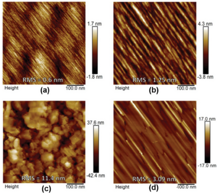
Figure 7 β-Ga2O3 (010) AFM image
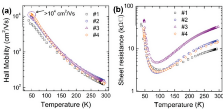
Figure 8 β-Ga2O3 The relationship betweenμand sheet resistance measured by Hall and temperature
2.3 HVPE method
HVPE is a mature epitaxial technology and has been widely used in the epitaxial growth of III-V compound semiconductors. HVPE is known for its low production cost, fast growth rate, and high film thickness. It should be noted that HVPEβ-Ga2O3 usually exhibits rough surface morphology and high density of surface defects and pits. Therefore, chemical and mechanical polishing processes are required before manufacturing the device. HVPE technology for β-Ga2O3 epitaxy usually uses gaseous GaCl and O2 as precursors to promote the high-temperature reaction of the (001) β-Ga2O3 matrix. Figure 9 shows the surface condition and growth rate of the epitaxial film as a function of temperature. In recent years, Japan’s Novel Crystal Technology Inc. has achieved significant commercial success in HVPE homoepitaxial β-Ga2O3, with epitaxial layer thicknesses of 5 to 10 μm and wafer sizes of 2 and 4 inches. In addition, 20 μm thick HVPE β-Ga2O3 homoepitaxial wafers produced by China Electronics Technology Group Corporation have also entered the commercialization stage.
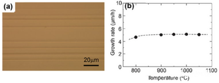
Figure 9 HVPE method β-Ga2O3
2.4 PLD method
PLD technology is mainly used to deposit complex oxide films and heterostructures. During the PLD growth process, photon energy is coupled to the target material through the electron emission process. In contrast to MBE, PLD source particles are formed by laser radiation with extremely high energy (>100 eV) and subsequently deposited on a heated substrate. However, during the ablation process, some high-energy particles will directly impact the material surface, creating point defects and thus reducing the quality of the film. Similar to the MBE method, RHEED can be used to monitor the surface structure and morphology of the material in real time during the PLD β-Ga2O3 deposition process, allowing researchers to accurately obtain growth information. The PLD method is expected to grow highly conductive β-Ga2O3 films, making it an optimized ohmic contact solution in Ga2O3 power devices.
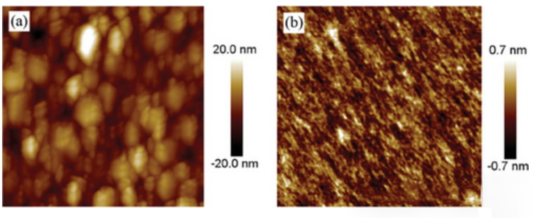
Figure 10 AFM image of Si doped Ga2O3
2.5 MIST-CVD method
MIST-CVD is a relatively simple and cost-effective thin film growth technology. This CVD method involves the reaction of spraying an atomized precursor onto a substrate to achieve thin film deposition. However, so far, Ga2O3 grown using mist CVD still lacks good electrical properties, which leaves a lot of room for improvement and optimization in the future.
Post time: May-30-2024