Wide bandgap (WBG) semiconductors represented by silicon carbide (SiC) and gallium nitride (GaN) have received widespread attention. People have high expectations for the application prospects of silicon carbide in electric vehicles and power grids, as well as the application prospects of gallium nitride in fast charging. In recent years, research on Ga2O3, AlN and diamond materials has made significant progress, making ultra-wide bandgap semiconductor materials the focus of attention. Among them, gallium oxide (Ga2O3) is an emerging ultra-wide-bandgap semiconductor material with a band gap of 4.8 eV, a theoretical critical breakdown field strength of about 8 MV cm-1, a saturation velocity of about 2E7cm s-1, and a high Baliga quality factor of 3000, receiving widespread attention in the field of high voltage and high frequency power electronics.
1. Gallium oxide material characteristics
Ga2O3 has a large band gap (4.8 eV), is expected to achieve both high withstand voltage and high power capabilities, and can have the potential for high voltage adaptability at relatively low resistance, making them the focus of current research. In addition, Ga2O3 not only has excellent material properties, but also provides a variety of easily adjustable n-type doping technologies, as well as low-cost substrate growth and epitaxy technologies. So far, five different crystal phases have been discovered in Ga2O3, including corundum (α), monoclinic (β), defective spinel (γ), cubic (δ) and orthorhombic (ɛ) phases. Thermodynamic stabilities are, in order, γ, δ, α, ɛ, and β. It is worth noting that monoclinic β-Ga2O3 is the most stable, especially at high temperatures, while other phases are metastable above room temperature and tend to transform into the β phase under specific thermal conditions. Therefore, the development of β-Ga2O3-based devices has become a major focus in the field of power electronics in recent years.
Table 1 Comparison of some semiconductor material parameters
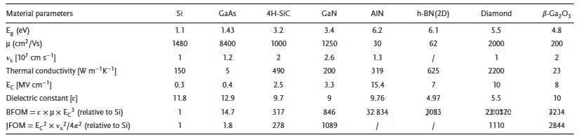
The crystal structure of monoclinicβ-Ga2O3 is shown in Table 1. Its lattice parameters include a = 12.21 Å, b = 3.04 Å, c = 5.8 Å, and β = 103.8°. The unit cell consists of Ga(I) atoms with twisted tetrahedral coordination and Ga(II) atoms with octahedral coordination. There are three different arrangements of oxygen atoms in the “twisted cubic” array, including two triangularly coordinated O(I) and O(II) atoms and one tetrahedrally coordinated O(III) atom. The combination of these two types of atomic coordination leads to the anisotropy of β-Ga2O3 with special properties in physics, chemical corrosion, optics and electronics.
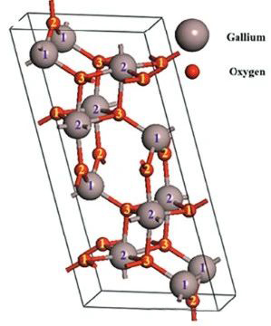
Figure 1 Schematic structural diagram of monoclinic β-Ga2O3 crystal
From the perspective of energy band theory, the minimum value of the conduction band of β-Ga2O3 is derived from the energy state corresponding to the 4s0 hybrid orbit of the Ga atom. The energy difference between the minimum value of the conduction band and the vacuum energy level (electron affinity energy) is measured. is 4 eV. The effective electron mass of β-Ga2O3 is measured as 0.28–0.33 me and its favorable electronic conductivity. However, the valence band maximum exhibits a shallow E-k curve with very low curvature and strongly localized O2p orbitals, suggesting that the holes are deeply localized. These characteristics pose a huge challenge to achieve p-type doping in β-Ga2O3. Even if P-type doping can be achieved, the hole μ remains at a very low level. 2. Growth of bulk gallium oxide single crystal So far, the growth method of β-Ga2O3 bulk single crystal substrate is mainly crystal pulling method, such as Czochralski (CZ), edge-defined thin film feeding method (Edge -Defined film-fed, EFG), Bridgman (rtical or horizontal Bridgman, HB or VB) and floating zone (floating zone, FZ) technology. Among all methods, Czochralski and edge-defined thin-film feeding methods are expected to be the most promising avenues for mass production of β-Ga 2O3 wafers in the future, as they can simultaneously achieve large volumes and low defect densities. Up to now, Japan’s Novel Crystal Technology has realized a commercial matrix for melt growth β-Ga2O3.
1.1 Czochralski method
The principle of Czochralski method is that the seed layer is first covered, and then the single crystal is slowly pulled out from the melt. The Czochralski method is increasingly important for β-Ga2O3 due to its cost-effectiveness, large size capabilities, and high crystal quality substrate growth. However, due to thermal stress during the high-temperature growth of Ga2O3, evaporation of single crystals, melt materials, and damage to the Ir crucible will occur. This is a result of the difficulty in achieving low n-type doping in Ga2O3. Introducing an appropriate amount of oxygen into the growth atmosphere is one way to solve this problem. Through optimization, high-quality 2-inch β-Ga2O3 with a free electron concentration range of 10^16~10^19 cm-3 and a maximum electron density of 160 cm2/Vs has been successfully grown by the Czochralski method.
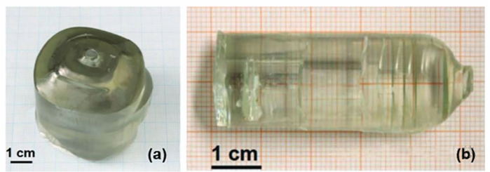
Figure 2 Single crystal of β-Ga2O3 grown by Czochralski method
1.2 Edge-defined film feeding method
The edge-defined thin film feeding method is considered to be the leading contender for the commercial production of large-area Ga2O3 single crystal materials. The principle of this method is to place the melt in a mold with a capillary slit, and the melt rises to the mold through capillary action. At the top, a thin film forms and spreads in all directions while being induced to crystallize by the seed crystal. Additionally, the edges of the mold top can be controlled to produce crystals in flakes, tubes, or any desired geometry. The edge-defined thin film feeding method of Ga2O3 provides fast growth rates and large diameters. Figure 3 shows a diagram of a β-Ga2O3 single crystal. In addition, in terms of size scale, 2-inch and 4-inch β-Ga2O3 substrates with excellent transparency and uniformity have been commercialized, while the 6-inch substrate is demonstrated in research for future commercialization. Recently, large circular single-crystal bulk materials have also become available with (−201) orientation. In addition, the β-Ga2O3 edge-defined film feeding method also promotes the doping of transition metal elements, making the research and preparation of Ga2O3 possible.
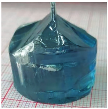
Figure 3 β-Ga2O3 single crystal grown by edge-defined film feeding method
1.3 Bridgeman method
In the Bridgeman method, crystals are formed in a crucible that is gradually moved through a temperature gradient. The process can be performed in a horizontal or vertical orientation, usually using a rotating crucible. It’s worth noting that this method may or may not use crystal seeds. Traditional Bridgman operators lack direct visualization of the melting and crystal growth processes and must control temperatures with high precision. The vertical Bridgman method is mainly used for the growth of β-Ga2O3 and is known for its ability to grow in an air environment. During the vertical Bridgman method growth process, the total mass loss of the melt and crucible is kept below 1%, enabling the growth of large β-Ga2O3 single crystals with minimal loss.
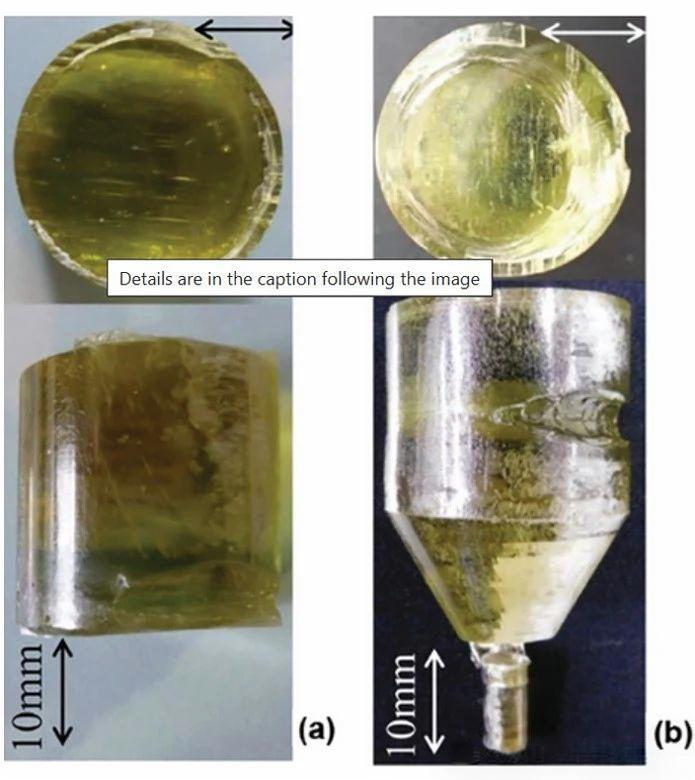
Figure 4 Single crystal of β-Ga2O3 grown by Bridgeman method
1.4 Floating zone method
The floating zone method solves the problem of crystal contamination by crucible materials and reduces the high costs associated with high temperature resistant infrared crucibles. During this growth process, the melt can be heated by a lamp rather than an RF source, thus simplifying the requirements for growth equipment. Although the shape and crystal quality of β-Ga2O3 grown by the floating zone method are not yet optimal, this method opens up a promising method for growing high-purity β-Ga2O3 into budget-friendly single crystals.
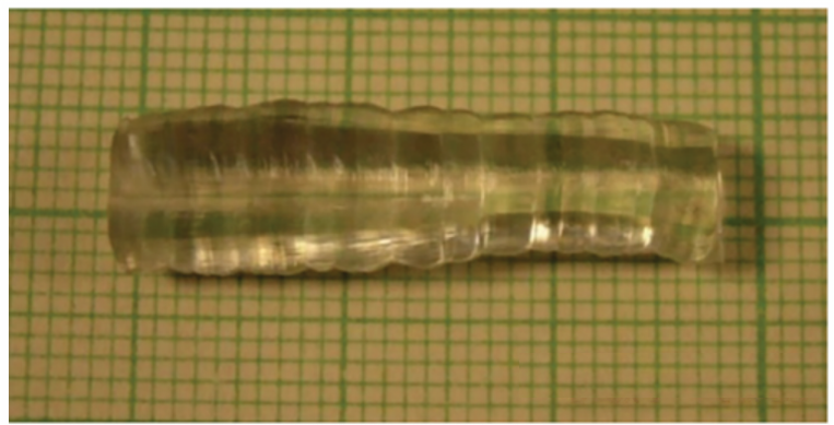
Figure 5 β-Ga2O3 single crystal grown by the floating zone method.
Post time: May-30-2024