Welcome to our website for product information and consultation.
Our website: https://www.vet-china.com/
As semiconductor manufacturing processes continue to make breakthroughs, a famous statement called "Moore's Law" has been circulating in the industry. It was proposed by Gordon Moore, one of the founders of Intel, in 1965. Its core content is: the number of transistors that can be accommodated on an integrated circuit will double approximately every 18 to 24 months. This law is not only an analysis and prediction of the development trend of the industry, but also a driving force for the development of semiconductor manufacturing processes - everything is to make transistors with smaller size and stable performance. From the 1950s to the present, about 70 years, a total of BJT, MOSFET, CMOS, DMOS, and hybrid BiCMOS and BCD process technologies have been developed.
1. BJT
Bipolar junction transistor (BJT), commonly known as triode. The charge flow in the transistor is mainly due to the diffusion and drift motion of carriers at the PN junction. Since it involves the flow of both electrons and holes, it is called a bipolar device.
Looking back at the history of its birth. Because of the idea of replacing vacuum triodes with solid amplifiers, Shockley proposed to carry out basic research on semiconductors in the summer of 1945. In the second half of 1945, Bell Labs established a solid-state physics research group headed by Shockley. In this group, there are not only physicists, but also circuit engineers and chemists, including Bardeen, a theoretical physicist, and Brattain, an experimental physicist. In December 1947, an event that was considered a milestone by later generations happened brilliantly - Bardeen and Brattain successfully invented the world's first germanium point-contact transistor with current amplification.
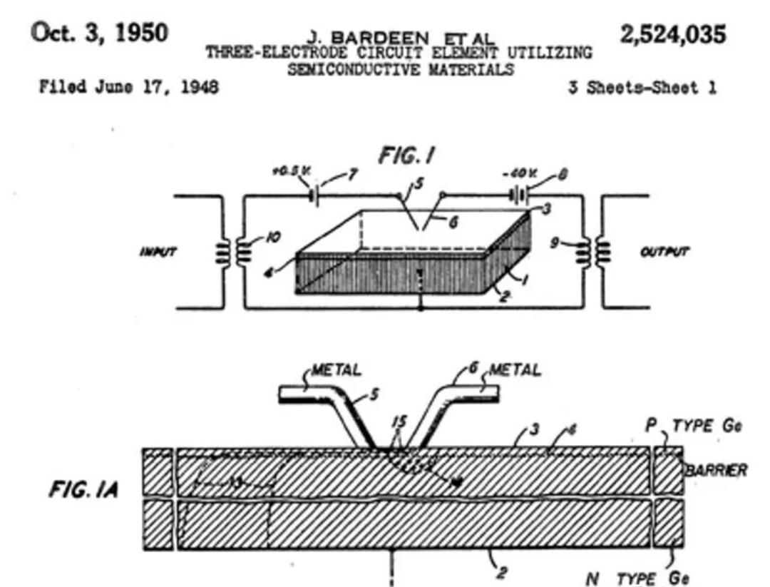
Bardeen and Brattain's first point-contact transistor
Shortly thereafter, Shockley invented the bipolar junction transistor in 1948. He proposed that the transistor can be composed of two pn junctions, one forward biased and the other reverse biased, and obtained a patent in June 1948. In 1949, he published the detailed theory of the working of the junction transistor. More than two years later, scientists and engineers at Bell Labs developed a process to achieve mass production of junction transistors (milestone in 1951), opening a new era of electronic technology. In recognition of their contributions to the invention of transistors, Shockley, Bardeen and Brattain jointly won the 1956 Nobel Prize in Physics.
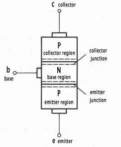
Simple structural diagram of NPN bipolar junction transistor
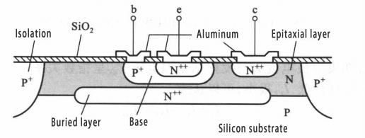
Regarding the structure of bipolar junction transistors, common BJTs are NPN and PNP. The detailed internal structure is shown in the figure below. The impurity semiconductor region corresponding to the emitter is the emitter region, which has a high doping concentration; the impurity semiconductor region corresponding to the base is the base region, which has a very thin width and a very low doping concentration; the impurity semiconductor region corresponding to the collector is the collector region, which has a large area and a very low doping concentration.
The advantages of BJT technology are high response speed, high transconductance (input voltage changes correspond to large output current changes), low noise, high analog accuracy, and strong current driving capability; the disadvantages are low integration (vertical depth cannot be reduced with lateral size) and high power consumption.
2. MOS
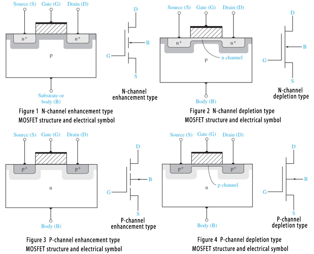
Metal Oxide Semiconductor Field Effect Transistor (Metal Oxide Semiconductor FET), that is, a field effect transistor that controls the switch of the semiconductor (S) conductive channel by applying voltage to the gate of the metal layer (M-metal aluminum) and the source through the oxide layer (O-insulating layer SiO2) to generate the effect of the electric field. Since the gate and the source, and the gate and the drain are isolated by the SiO2 insulating layer, MOSFET is also called an insulated gate field effect transistor. In 1962, Bell Labs officially announced the successful development, which became one of the most important milestones in the history of semiconductor development and directly laid the technical foundation for the advent of semiconductor memory.
MOSFET can be divided into P channel and N channel according to the conductive channel type. According to the gate voltage amplitude, it can be divided into: depletion type-when the gate voltage is zero, there is a conductive channel between the drain and the source; enhancement type-for N (P) channel devices, there is a conductive channel only when the gate voltage is greater than (less than) zero, and power MOSFET is mainly N channel enhancement type.
The main differences between MOS and triode include but are not limited to the following points:
-Triodes are bipolar devices because both majority and minority carriers participate in conduction at the same time; while MOS only conducts electricity through majority carriers in semiconductors, and is also called a unipolar transistor.
-Triodes are current-controlled devices with relatively high power consumption; while MOSFETs are voltage-controlled devices with low power consumption.
-Triodes have large on-resistance, while MOS tubes have small on-resistance, only a few hundred milliohms. In current electrical devices, MOS tubes are generally used as switches, mainly because the efficiency of MOS is relatively high compared to triodes.
-Triodes have a relatively advantageous cost, and MOS tubes are relatively expensive.
-Nowadays, MOS tubes are used to replace triodes in most scenarios. Only in some low-power or power-insensitive scenarios, we will use triodes considering the price advantage.
3. CMOS
Complementary Metal Oxide Semiconductor: CMOS technology uses complementary p-type and n-type metal oxide semiconductor transistors (MOSFETs) to build electronic devices and logic circuits. The following figure shows a common CMOS inverter, which is used for "1→0" or "0→1" conversion.
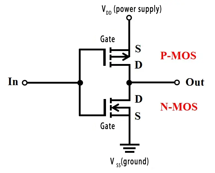
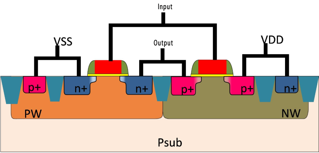
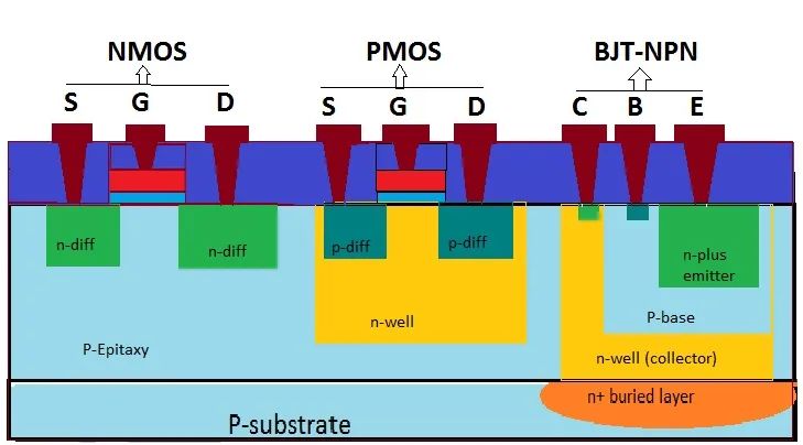
The following figure is a typical CMOS cross-section. The left side is NMS, and the right side is PMOS. The G poles of the two MOS are connected together as a common gate input, and the D poles are connected together as a common drain output. VDD is connected to the source of PMOS, and VSS is connected to the source of NMOS.
In 1963, Wanlass and Sah of Fairchild Semiconductor invented the CMOS circuit. In 1968, the American Radio Corporation (RCA) developed the first CMOS integrated circuit product, and since then, the CMOS circuit has achieved great development. Its advantages are low power consumption and high integration (STI/LOCOS process can further improve integration); its disadvantage is the existence of a lock effect (PN junction reverse bias is used as isolation between MOS tubes, and interference can easily form an enhanced loop and burn the circuit).
4. DMOS
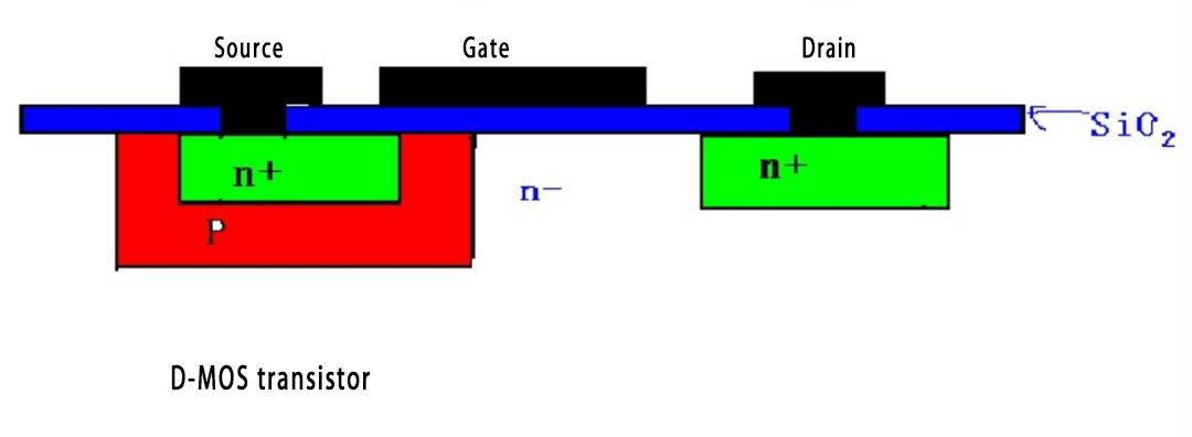
Double-Diffused Metal Oxide Semiconductor: Similar to the structure of ordinary MOSFET devices, it also has source, drain, gate and other electrodes, but the breakdown voltage of the drain end is high. Double diffusion process is used.
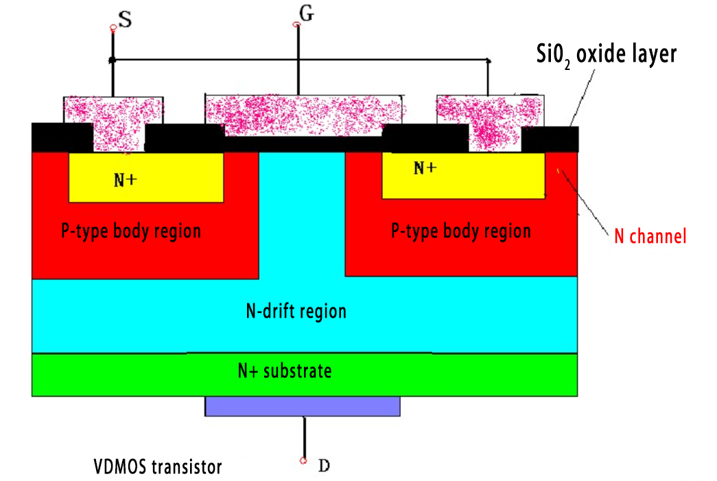
The figure below shows the cross-section of a standard N-channel DMOS. This type of DMOS device is usually used in low-side switching applications, where the source of the MOSFET is connected to the ground. In addition, there is a P-channel DMOS. This type of DMOS device is usually used in high-side switching applications, where the source of the MOSFET is connected to a positive voltage. Similar to CMOS, complementary DMOS devices use N-channel and P-channel MOSFETs on the same chip to provide complementary switching functions.
Depending on the direction of the channel, DMOS can be divided into two types, namely vertical double-diffused metal oxide semiconductor field effect transistor VDMOS (Vertical Double-Diffused MOSFET) and lateral double-diffused metal oxide semiconductor field effect transistor LDMOS (Lateral Double-Diffused MOSFET).
VDMOS devices are designed with a vertical channel. Compared with lateral DMOS devices, they have higher breakdown voltage and current handling capabilities, but the on-resistance is still relatively large.
LDMOS devices are designed with a lateral channel and are asymmetric power MOSFET devices. Compared with vertical DMOS devices, they allow lower on-resistance and faster switching speeds.
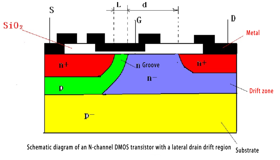
Compared with traditional MOSFETs, DMOS has higher on-capacitance and lower resistance, so it is widely used in high-power electronic devices such as power switches, power tools and electric vehicle drives.
5. BiCMOS
Bipolar CMOS is a technology that integrates CMOS and bipolar devices on the same chip at the same time. Its basic idea is to use CMOS devices as the main unit circuit, and add bipolar devices or circuits where large capacitive loads are required to be driven. Therefore, BiCMOS circuits have the advantages of high integration and low power consumption of CMOS circuits, and the advantages of high speed and strong current driving capabilities of BJT circuits.
STMicroelectronics' BiCMOS SiGe (silicon germanium) technology integrates RF, analog and digital parts on a single chip, which can significantly reduce the number of external components and optimize power consumption.
6. BCD
Bipolar-CMOS-DMOS, this technology can make bipolar, CMOS and DMOS devices on the same chip, called BCD process, which was first successfully developed by STMicroelectronics (ST) in 1986.
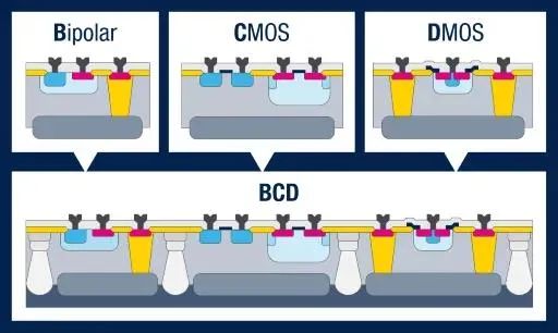
Bipolar is suitable for analog circuits, CMOS is suitable for digital and logic circuits, and DMOS is suitable for power and high-voltage devices. BCD combines the advantages of the three. After continuous improvement, BCD is widely used in products in the fields of power management, analog data acquisition and power actuators. According to ST's official website, the mature process for BCD is still around 100nm, 90nm is still in prototype design, and 40nmBCD technology belongs to its next-generation products under development.
Post time: Sep-10-2024