What is BCD process?
BCD process is a single-chip integrated process technology first introduced by ST in 1986. This technology can make bipolar, CMOS and DMOS devices on the same chip. Its appearance greatly reduces the area of the chip.
It can be said that the BCD process fully utilizes the advantages of Bipolar driving capability, CMOS high integration and low power consumption, and DMOS high voltage and high current flow capacity. Among them, DMOS is the key to improving power and integration. With the further development of integrated circuit technology, BCD process has become the mainstream manufacturing technology of PMIC.
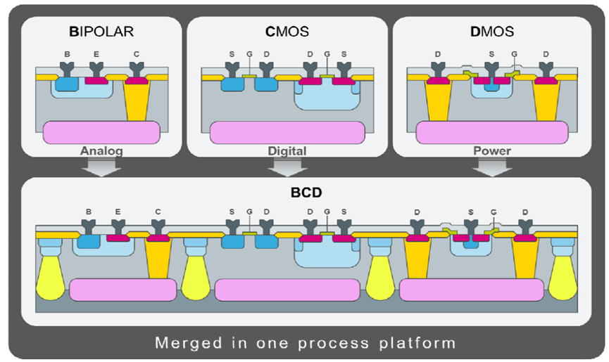
BCD process cross-sectional diagram, source network, thank you
Advantages of BCD process
BCD process makes Bipolar devices, CMOS devices, and DMOS power devices on the same chip at the same time, integrating the high transconductance and strong load driving capability of bipolar devices and the high integration and low power consumption of CMOS, so that they can complement each other and give full play to their respective advantages; at the same time, DMOS can work in switching mode with extremely low power consumption. In short, low power consumption, high energy efficiency and high integration are one of the main advantages of BCD. BCD process can significantly reduce power consumption, improve system performance and have better reliability. The functions of electronic products are increasing day by day, and the requirements for voltage changes, capacitor protection and battery life extension are becoming increasingly important. The high-speed and energy-saving characteristics of BCD meet the process requirements for high-performance analog/power management chips.
Key technologies of BCD process
Typical devices of BCD process include low-voltage CMOS, high-voltage MOS tubes, LDMOS with various breakdown voltages, vertical NPN/PNP and Schottky diodes, etc. Some processes also integrate devices such as JFET and EEPROM, resulting in a large variety of devices in BCD process. Therefore, in addition to considering the compatibility of high-voltage devices and low-voltage devices, double-click processes and CMOS processes, etc. in the design, appropriate isolation technology must also be considered.
In BCD isolation technology, many technologies such as junction isolation, self-isolation and dielectric isolation have emerged one after another. Junction isolation technology is to make the device on the N-type epitaxial layer of the P-type substrate and use the reverse bias characteristics of the PN junction to achieve isolation, because the PN junction has a very high resistance under reverse bias.
Self-isolation technology is essentially PN junction isolation, which relies on the natural PN junction characteristics between the source and drain regions of the device and the substrate to achieve isolation. When the MOS tube is turned on, the source region, drain region and channel are surrounded by the depletion region, forming isolation from the substrate. When it is turned off, the PN junction between the drain region and the substrate is reverse biased, and the high voltage of the source region is isolated by the depletion region.
Dielectric isolation uses insulating media such as silicon oxide to achieve isolation. Based on dielectric isolation and junction isolation, quasi-dielectric isolation has been developed by combining the advantages of both. By selectively adopting the above isolation technology, high-voltage and low-voltage compatibility can be achieved.
Development direction of BCD process
The development of BCD process technology is not like the standard CMOS process, which has always followed Moore’s law to develop in the direction of smaller line width and faster speed. BCD process is roughly differentiated and developed in three directions: high voltage, high power, and high density.
1. High-voltage BCD direction
High-voltage BCD can manufacture high-reliability low-voltage control circuits and ultra-high-voltage DMOS-level circuits on the same chip at the same time, and can realize the production of 500-700V high-voltage devices. However, in general, BCD is still suitable for products with relatively high requirements for power devices, especially BJT or high-current DMOS devices, and can be used for power control in electronic lighting and industrial applications.
The current technology for manufacturing high-voltage BCD is the RESURF technology proposed by Appel et al. in 1979. The device is made using a lightly doped epitaxial layer to make the surface electric field distribution flatter, thereby improving the surface breakdown characteristics, so that the breakdown occurs in the body instead of the surface, thereby increasing the device’s breakdown voltage. Light doping is another method to increase the breakdown voltage of BCD. It mainly uses double diffused drain DDD (double Doping Drain) and lightly doped drain LDD (lightly Doping Drain). In the DMOS drain region, an N-type drift region is added to change the original contact between the N+ drain and the P-type substrate to the contact between the N- drain and the P-type substrate, thereby increasing the breakdown voltage.
2. High-power BCD direction
The voltage range of high-power BCD is 40-90V, and it is mainly used in automotive electronics that require high current driving capability, medium voltage and simple control circuits. Its demand characteristics are high current driving capability, medium voltage, and the control circuit is often relatively simple.
3. High-density BCD direction
High-density BCD, the voltage range is 5-50V, and some automotive electronics will reach 70V. More and more complex and diverse functions can be integrated on the same chip. High-density BCD adopts some modular design ideas to achieve product diversification, mainly used in automotive electronics applications.
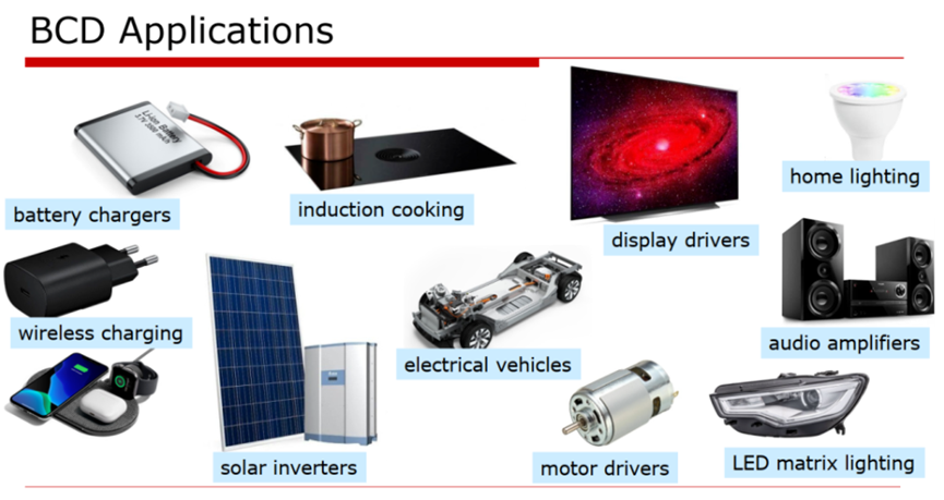
Main applications of BCD process
BCD process is widely used in power management (power and battery control), display drive, automotive electronics, industrial control, etc. Power management chip (PMIC) is one of the important types of analog chips. The combination of BCD process and SOI technology is also a major feature of the development of BCD process.
VET-China can provide graphite parts, softrigid felt, silicon carbide parts, cvD silicon carbide parts, and sic/Tac coated partswith in 30 days.
If you are interested in the above semiconductor products, please do not hesitate to contact us at the first time.
Tel:+86-1891 1596 392
WhatsAPP:86-18069021720
Email:yeah@china-vet.com
Post time: Sep-18-2024