Thin film deposition is to coat a layer of film on the main substrate material of the semiconductor. This film can be made of various materials, such as insulating compound silicon dioxide, semiconductor polysilicon, metal copper, etc. The equipment used for coating is called thin film deposition equipment.
From the perspective of the semiconductor chip manufacturing process, it is located in the front-end process.

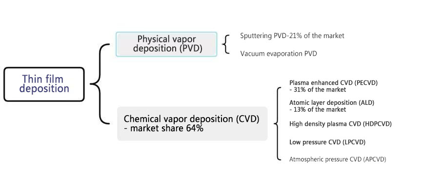
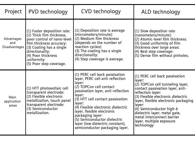
The thin film preparation process can be divided into two categories according to its film forming method: physical vapor deposition (PVD) and chemical vapor deposition (CVD), among which CVD process equipment accounts for a higher proportion.
Physical vapor deposition (PVD) refers to the vaporization of the surface of the material source and deposition on the surface of the substrate through low-pressure gas/plasma, including evaporation, sputtering, ion beam, etc.;
Chemical vapor deposition (CVD) refers to the process of depositing a solid film on the surface of the silicon wafer through a chemical reaction of gas mixture. According to the reaction conditions (pressure, precursor), it is divided into atmospheric pressure CVD (APCVD), low pressure CVD (LPCVD), plasma enhanced CVD (PECVD), high density plasma CVD (HDPCVD) and atomic layer deposition (ALD).
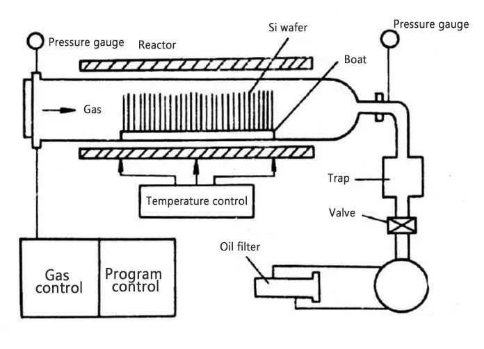
LPCVD: LPCVD has better step coverage ability, good composition and structure control, high deposition rate and output, and greatly reduces the source of particle pollution. Relying on heating equipment as a heat source to maintain the reaction, temperature control and gas pressure are very important. Widely used in the Poly layer manufacturing of TopCon cells.
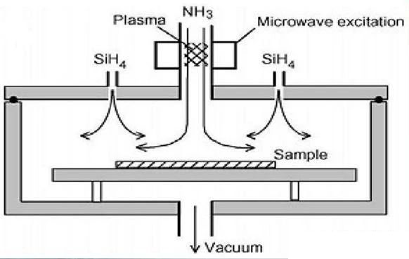
PECVD: PECVD relies on the plasma generated by radio frequency induction to achieve low temperature (less than 450 degrees) of the thin film deposition process. Low temperature deposition is its main advantage, thereby saving energy, reducing costs, increasing production capacity, and reducing the lifetime decay of minority carriers in silicon wafers caused by high temperature. It can be applied to the processes of various cells such as PERC, TOPCON, and HJT.
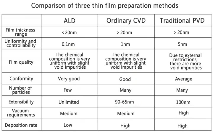
ALD: Good film uniformity, dense and without holes, good step coverage characteristics, can be carried out at low temperature (room temperature-400℃), can simply and accurately control the film thickness, is widely applicable to substrates of different shapes, and does not need to control the uniformity of the reactant flow. But the disadvantage is that the film formation speed is slow. Such as the zinc sulfide (ZnS) light-emitting layer used to produce nanostructured insulators (Al2O3/TiO2) and thin-film electroluminescent displays (TFEL).
Atomic layer deposition (ALD) is a vacuum coating process that forms a thin film on the surface of a substrate layer by layer in the form of a single atomic layer. As early as 1974, Finnish material physicist Tuomo Suntola developed this technology and won the 1 million euro Millennium Technology Award. ALD technology was originally used for flat-panel electroluminescent displays, but it was not widely used. It was not until the beginning of the 21st century that ALD technology began to be adopted by the semiconductor industry. By manufacturing ultra-thin high-dielectric materials to replace traditional silicon oxide, it successfully solved the leakage current problem caused by the reduction of line width of field effect transistors, prompting Moore’s Law to further develop towards smaller line widths. Dr. Tuomo Suntola once said that ALD can significantly increase the integration density of components.
Public data shows that ALD technology was invented by Dr. Tuomo Suntola of PICOSUN in Finland in 1974 and has been industrialized abroad, such as the high dielectric film in the 45/32 nanometer chip developed by Intel. In China, my country introduced ALD technology more than 30 years later than foreign countries. In October 2010, PICOSUN in Finland and Fudan University hosted the first domestic ALD academic exchange meeting, introducing ALD technology to China for the first time.
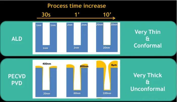
Compared with traditional chemical vapor deposition (CVD) and physical vapor deposition (PVD), the advantages of ALD are excellent three-dimensional conformality, large-area film uniformity, and precise thickness control, which are suitable for growing ultra-thin films on complex surface shapes and high aspect ratio structures.
—Data source: Micro-nano processing platform of Tsinghua University—
In the post-Moore era, the complexity and process volume of wafer manufacturing have been greatly improved. Taking logic chips as an example, with the increase in the number of production lines with processes below 45nm, especially the production lines with processes of 28nm and below, the requirements for coating thickness and precision control are higher. After the introduction of multiple exposure technology, the number of ALD process steps and equipment required have increased significantly; in the field of memory chips, the mainstream manufacturing process has evolved from 2D NAND to 3D NAND structure, the number of internal layers has continued to increase, and the components have gradually presented high-density, high aspect ratio structures, and the important role of ALD has begun to emerge. From the perspective of the future development of semiconductors, ALD technology will play an increasingly important role in the post-Moore era.
For example, ALD is the only deposition technology that can meet the coverage and film performance requirements of complex 3D stacked structures (such as 3D-NAND). This can be vividly seen in the figure below. The film deposited in CVD A (blue) does not completely cover the lower part of the structure; even if some process adjustments are made to CVD (CVD B) to achieve coverage, the film performance and chemical composition of the bottom area are very poor (white area in the figure); in contrast, the use of ALD technology shows complete film coverage, and high-quality and uniform film properties are achieved in all areas of the structure.
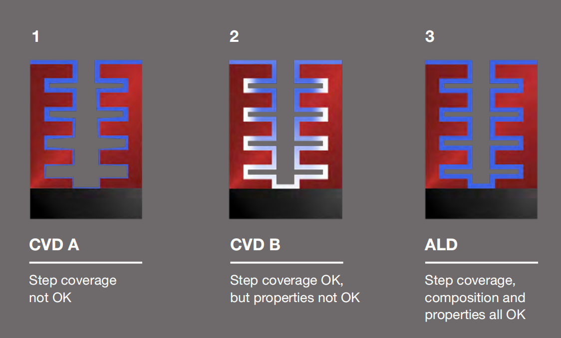
—-Picture Advantages of ALD technology compared to CVD (Source: ASM)—-
Although CVD still occupies the largest market share in the short term, ALD has become one of the fastest growing parts of the wafer fab equipment market. In this ALD market with great growth potential and a key role in chip manufacturing, ASM is a leading company in the field of ALD equipment.
Post time: Jun-12-2024