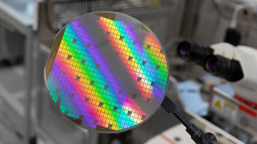
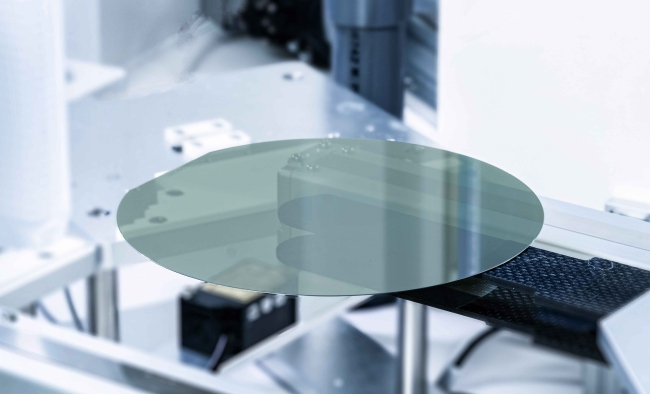
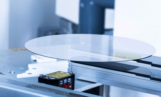
The Monocrystalline 8 Inch Silicon Wafer from VET Energy is an industry-leading solution for semiconductor and electronic device fabrication. Offering superior purity and crystalline structure, these wafers are ideal for high-performance applications in both the photovoltaic and semiconductor industries. VET Energy ensures that every wafer is meticulously processed to meet the highest standards, providing excellent uniformity and smooth surface finish, which are essential for advanced electronic device production.
These Monocrystalline 8 Inch Silicon Wafers are compatible with a range of materials, including Si Wafer, SiC Substrate, SOI Wafer, SiN Substrate, and are particularly suited for Epi Wafer growth. Their superior thermal conductivity and electrical properties make them a reliable choice for high-efficiency manufacturing. Additionally, these wafers are designed to work seamlessly with materials such as Gallium Oxide Ga2O3 and AlN Wafer, offering a wide range of applications from power electronics to RF devices. The wafers also fit perfectly into Cassette systems for high-volume, automated production environments.
VET Energy's product line is not limited to silicon wafers. We also provide a wide range of semiconductor substrate materials, including SiC Substrate, SOI Wafer, SiN Substrate, Epi Wafer, etc., as well as new wide bandgap semiconductor materials such as Gallium Oxide Ga2O3 and AlN Wafer. These products can meet the application needs of different customers in power electronics, radio frequency, sensors and other fields.
VET Energy provides customers with customized wafer solutions. We can customize wafers with different resistivity, oxygen content, thickness, etc. according to customers' specific needs. In addition, we also provide professional technical support and after-sales service to help customers solve various problems encountered during the production process.
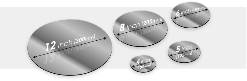
WAFERING SPECIFICATIONS
*n-Pm=n-type Pm-Grade,n-Ps=n-type Ps-Grade,Sl=Semi-lnsulating
|
Item |
8-Inch |
6-Inch |
4-Inch |
||
|
n-P |
n-Pm |
n-Ps |
SI |
SI |
|
|
TTV(GBIR) |
≤6um |
≤6um |
|||
|
Bow(GF3YFCD)-Absolute Value |
≤15μm |
≤15μm |
≤25μm |
≤15μm |
|
|
Warp(GF3YFER) |
≤25μm |
≤25μm |
≤40μm |
≤25μm |
|
|
LTV(SBIR)-10mmx10mm |
<2μm |
||||
|
Wafer Edge |
Beveling |
||||
SURFACE FINISH
*n-Pm=n-type Pm-Grade,n-Ps=n-type Ps-Grade,Sl=Semi-lnsulating
|
Item |
8-Inch |
6-Inch |
4-Inch |
||
|
n-P |
n-Pm |
n-Ps |
SI |
SI |
|
|
Surface Finish |
Double side Optical Polish,Si- Face CMP |
||||
|
SurfaceRoughness |
(10um x 10um) Si-FaceRa≤0.2nm |
(5umx5um) Si-Face Ra≤0.2nm |
|||
|
Edge Chips |
None Permitted (length and width≥0.5mm) |
||||
|
Indents |
None Permitted |
||||
|
Scratches(Si-Face) |
Qty.≤5,Cumulative |
Qty.≤5,Cumulative |
Qty.≤5,Cumulative |
||
|
Cracks |
None Permitted |
||||
|
Edge Exclusion |
3mm |
||||