We continue to keep increasing and perfecting our solutions and service. At the same time, we operate actively to do research and enhancement for Lowest Price for China High Quality Customized Graphite Heater for Polycrystalline Silicon Ingot Furnace, Our enterprise quickly grew in size and popularity because of its absolute dedication to top quality manufacturing, large price of products and fantastic customer provider.
We continue to keep increasing and perfecting our solutions and service. At the same time, we operate actively to do research and enhancement for China Graphite Heating Furnace, Graphite Thermal Field, Only for accomplishing the good-quality product to meet customer’s demand, all of our products and solutions have been strictly inspected before shipment. We always think about the question on the side of the customers, because you win, we win!
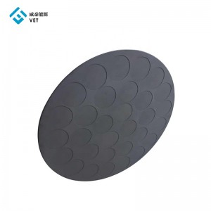
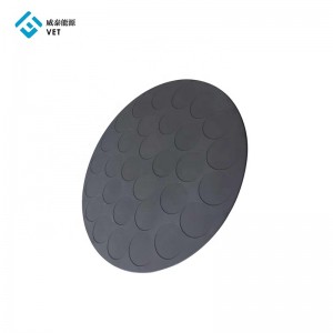
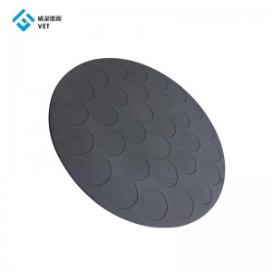
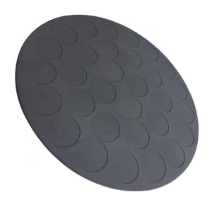
2022 high quality MOCVD Susceptor Buy online in China
| Apparent Density: | 1.85 g/cm3 |
| Electrical Resistivity: | 11 μΩm |
| Flexural Strenth: | 49 MPa (500kgf/cm2) |
| Shore Hardness: | 58 |
| Ash: | <5ppm |
| Thermal Conductivity: | 116 W/mK (100 kcal/mhr-℃) |
A wafer is a slice of silicon roughly 1 millimeter thick that has an extremely flat surface thanks to procedures that are technically very demanding. The subsequent use determines which crystal growing procedure should be employed. In the Czochralski process, for example, the polycrystalline silicon is melted and a pencil-thin seed crystal is dipped into the molten silicon. The seed crystal is then rotated and slowly pulled upwards. A very heavy colossus, a monocrystal, results. It is possible to select the monocrystal’s electrical characteristics by adding small units of high-purity dopants. The crystals are doped in accordance with the customer specifications and then polished and cut into slices. After various additional production steps, the customer receives its specified wafers in special packaging, which allows the customer to use the wafer immediately in its production line.
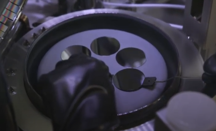
A wafer needs to pass through several steps before it is ready for use in electronic devices. One important process is silicon epitaxy, in which the wafers are carried on graphite susceptors. The properties and quality of the susceptors have a crucial effect on the quality of the wafer’s epitaxial layer.
For thin film deposition phases such as epitaxy or MOCVD, VET supplies ultra-pure graphiteequipment used to support substrates or “wafers”. At the core of the process, this equipment, epitaxy susceptors or satellite platforms for the MOCVD, are first subjected to the deposition environment:
High temperature.
High vacuum.
Use of aggressive gaseous precursors.
Zero contamination, absence of peeling.
Resistance to strong acids during cleaning operations
-
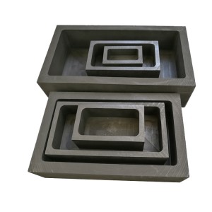
Customized Metal Melting SIC Ingot Mould,Silico...
-

CVD SiC Coated Carbon-carbon Composite CFC Boat...
-
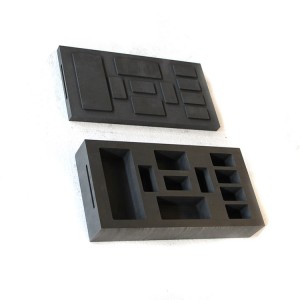
CVD sic coating carbon-carbon composite mould
-
Carbon-carbon Composite Plate With SiC Coating
-
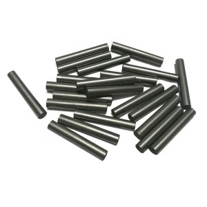
CVD sic coating c-c composite rod,silicon carbi...
-
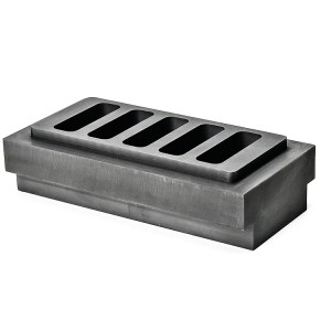
gold and silver castiong mould Silicon Mould,Si...
-

Gold Silver Melting Graphite Crucible Graphite Pot
-

High quality Silicon rod,Sic rod for processing...
-
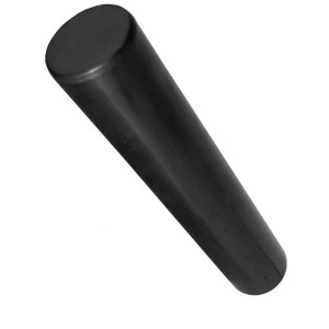
High temperature resistance durable Silicon rod...
-
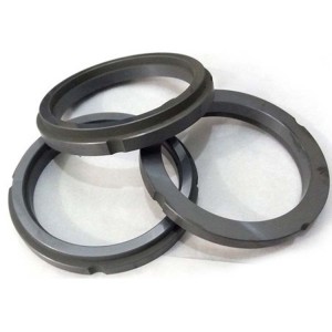
Mechanical Carbon Graphite Bush Rings,Silicone ...
-
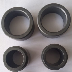
oil resistance SIC thrust bearing,Silicon bearing
-
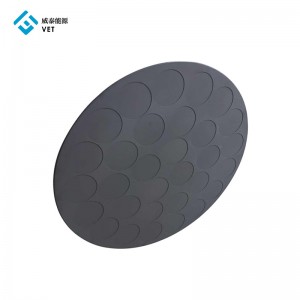
SiC Coated Graphite Base Carriers
-
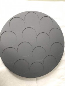
Silicon Carbide Coated Graphite Substrate for S...
-
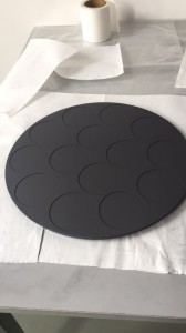
Graphite Substrates/Carriers with Silicon Carbi...
-
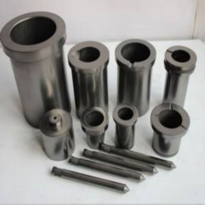
Graphite crucible for melting aluminum copper g...


