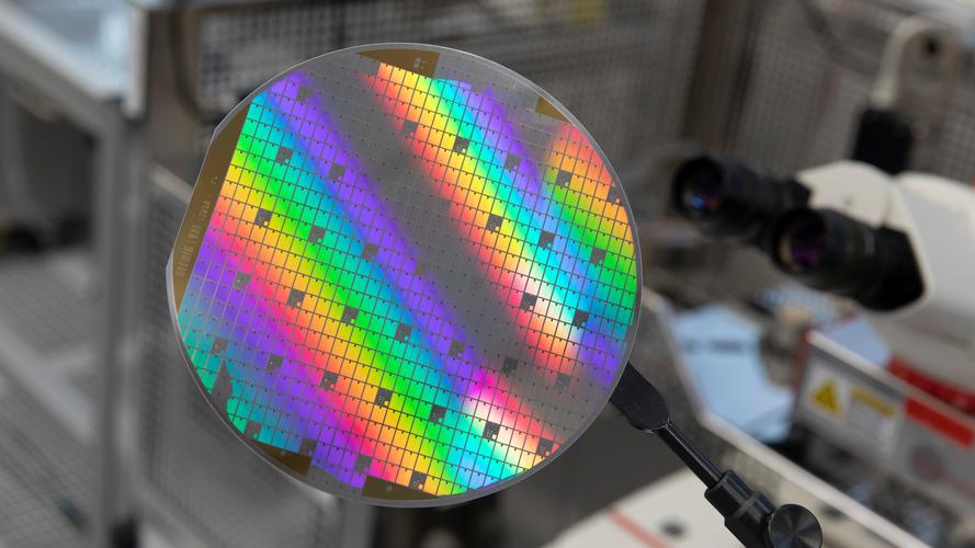
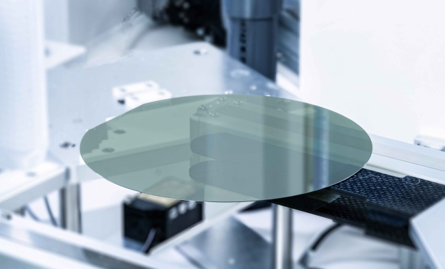
VET Energy's 8-inch silicon wafers are widely used in power electronics, sensors, integrated circuits and other fields. As a leader in the semiconductor industry, we are committed to providing high-quality Si Wafer products to meet the growing needs of our customers.
In addition to Si Wafer, VET Energy also provides a wide range of semiconductor substrate materials, including SiC Substrate, SOI Wafer, SiN Substrate, Epi Wafer, etc. Our product line also covers new wide bandgap semiconductor materials such as Gallium Oxide Ga2O3 and AlN Wafer, providing strong support for the development of next-generation power electronic devices.
VET Energy has advanced production equipment and a complete quality management system to ensure that each wafer meets strict industry standards. Our products not only have excellent electrical properties, but also have good mechanical strength and thermal stability.
VET Energy provides customers with customized wafer solutions, including wafers of different sizes, types and doping concentrations. In addition, we also provide professional technical support and after-sales service to help customers solve various problems encountered during the production process.

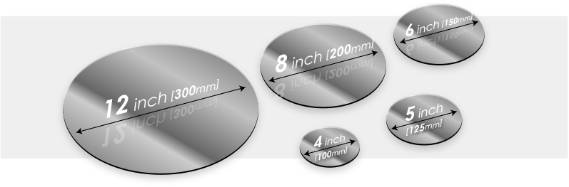
WAFERING SPECIFICATIONS
*n-Pm=n-type Pm-Grade,n-Ps=n-type Ps-Grade,Sl=Semi-lnsulating
|
Item |
8-Inch |
6-Inch |
4-Inch |
||
|
n-P |
n-Pm |
n-Ps |
SI |
SI |
|
|
TTV(GBIR) |
≤6um |
≤6um |
|||
|
Bow(GF3YFCD)-Absolute Value |
≤15μm |
≤15μm |
≤25μm |
≤15μm |
|
|
Warp(GF3YFER) |
≤25μm |
≤25μm |
≤40μm |
≤25μm |
|
|
LTV(SBIR)-10mmx10mm |
<2μm |
||||
|
Wafer Edge |
Beveling |
||||
SURFACE FINISH
*n-Pm=n-type Pm-Grade,n-Ps=n-type Ps-Grade,Sl=Semi-lnsulating
|
Item |
8-Inch |
6-Inch |
4-Inch |
||
|
n-P |
n-Pm |
n-Ps |
SI |
SI |
|
|
Surface Finish |
Double side Optical Polish,Si- Face CMP |
||||
|
SurfaceRoughness |
(10um x 10um) Si-FaceRa≤0.2nm |
(5umx5um) Si-Face Ra≤0.2nm |
|||
|
Edge Chips |
None Permitted (length and width≥0.5mm) |
||||
|
Indents |
None Permitted |
||||
|
Scratches(Si-Face) |
Qty.≤5,Cumulative |
Qty.≤5,Cumulative |
Qty.≤5,Cumulative |
||
|
Cracks |
None Permitted |
||||
|
Edge Exclusion |
3mm |
||||