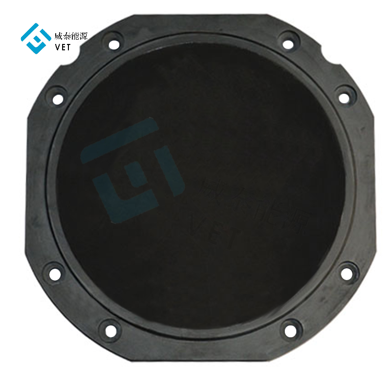
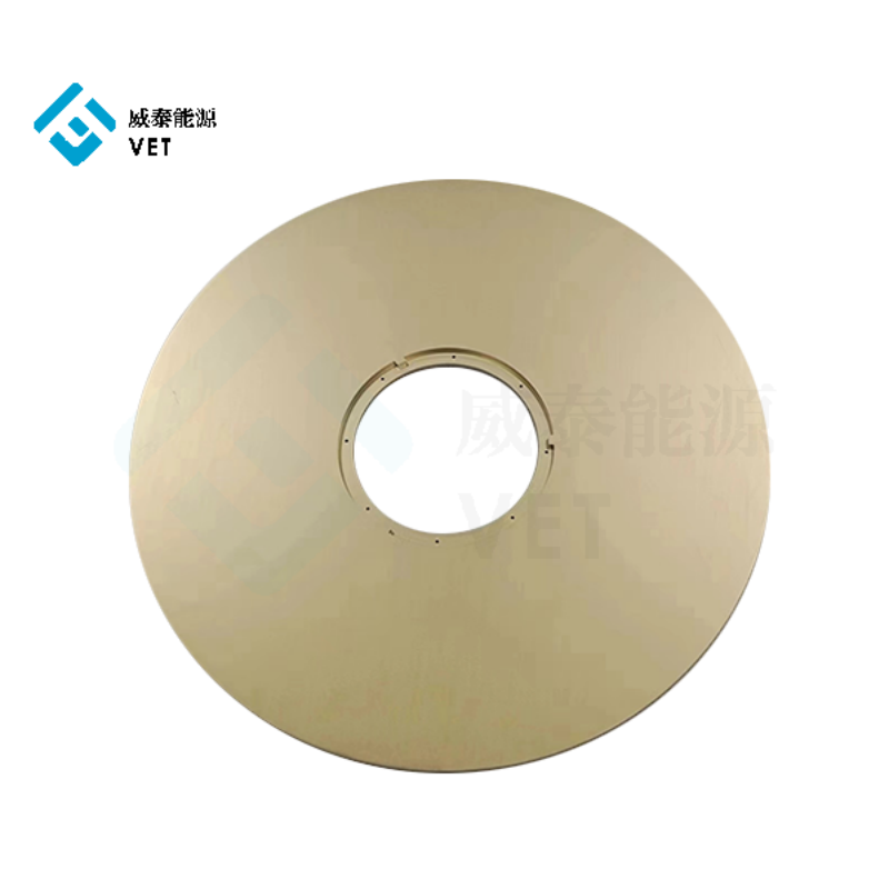
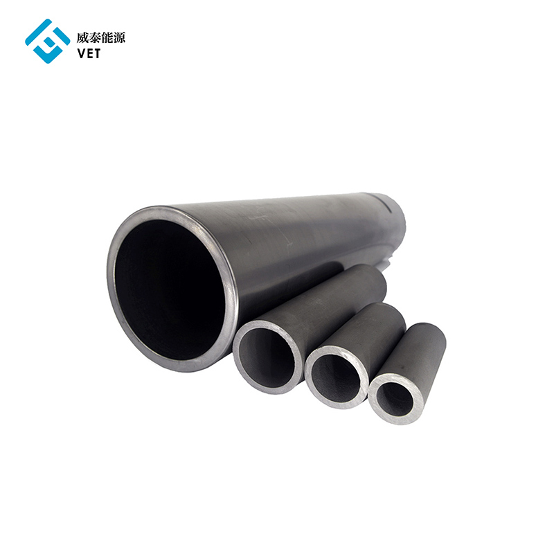
Thin film deposition is to coat a layer of film on the main substrate material of the semiconductor. This film can be made of various materials, such as insulating compound silicon dioxide, semicon...
Textured Cu substrates are composed of three layers (thickness of 0.1mm, width of 10mm) (Photo: Business Wire)
Textured Cu substrates are composed of three layers (thickness of 0.1mm, width of 10mm...
The bond could not be resold for interest, and the A-share market was again thundering.
On November 19, Dongxu Optoelectronics announced a debt default.
On the 19th, Dongxu Optoelectronics and Dong...
Some organic and inorganic substances are required to participate in semiconductor manufacturing. In addition, since the process is always carried out in a clean room with human participation, semi...
Industrially, natural graphite is classified into crystalline graphite and cryptocrystalline graphite according to the crystal form. The crystalline graphite is better crystallized, and the crystal...
West Lafayette, Indiana – SK hynix Inc. announced plans to invest nearly $4 billion to build an advanced packaging manufacturing and R&D facility for artificial intelligence products at P...