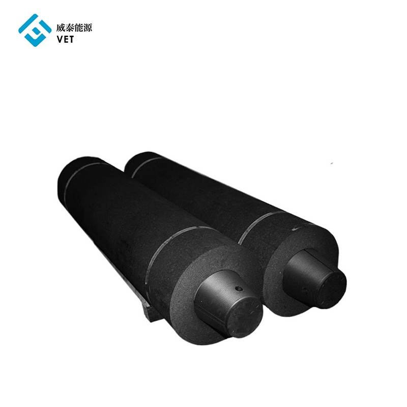
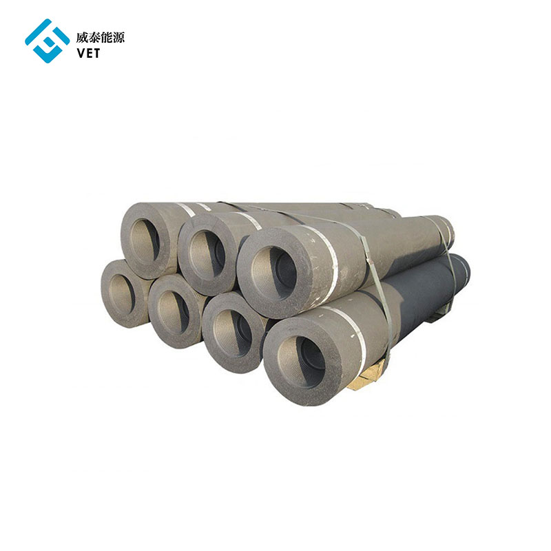
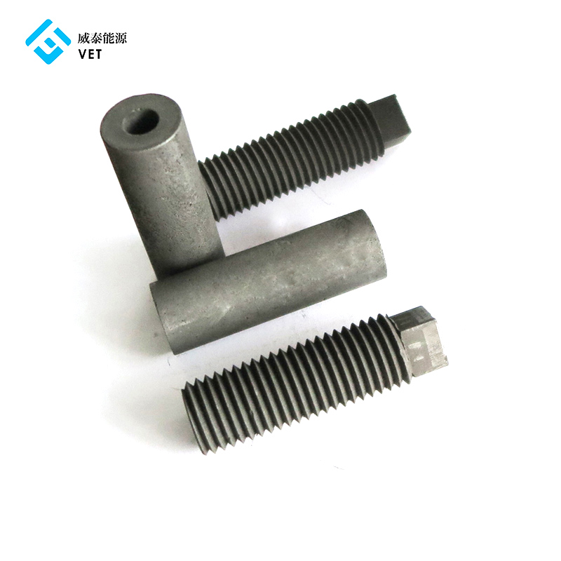
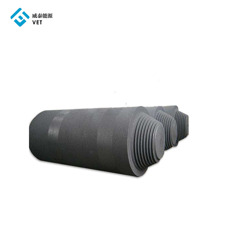
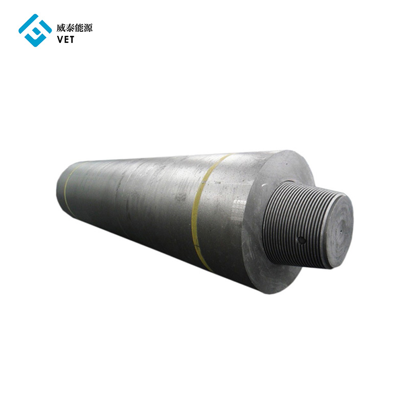
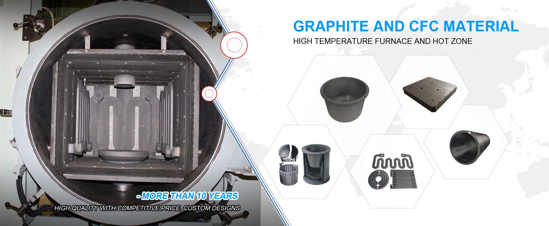
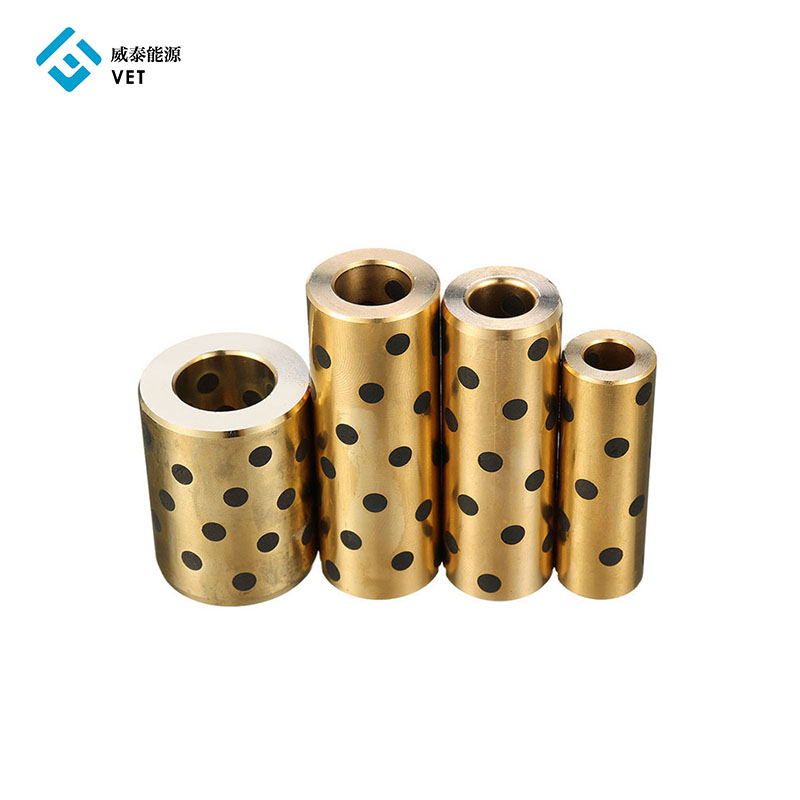
HOW TO MAKE A SILICON WAFER
A wafer is a slice of silicon roughly 1 millimeter thick that has an extremely flat surface thanks to procedures that are technically very demanding. The subsequent use ...
Sichuan Province is vast in area and rich in mineral resources. Among them, the prospecting potential of emerging strategic resources is huge. A few days ago, it was led by Sichuan Natural Resourc...
Tantalum carbide hardness, high melting point, high temperature performance, mainly used as a hard alloy additive. The thermal hardness, thermal shock resistance and thermal oxidation resistance of...
Industrially, natural graphite is classified into crystalline graphite and cryptocrystalline graphite according to the crystal form. The crystalline graphite is better crystallized, and the crystal...
The market research report recently added to the “Trusted Market” repository is an in-depth analysis of the global carbon-graphite brush market. The report is based on historical growth...
In the back-end process stage, the wafer (silicon wafer with circuits on the front) needs to be thinned on the back before subsequent dicing, welding and packaging to reduce the package mounting he...