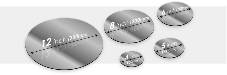
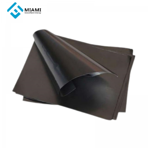
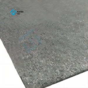
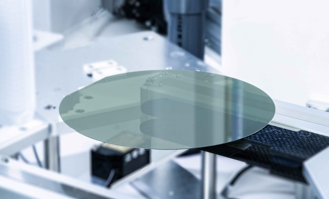
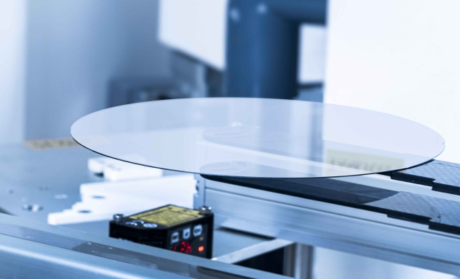
The 6 Inch Semi Insulating SiC Wafer from VET Energy is an advanced solution for high-power and high-frequency applications, offering superior thermal conductivity and electrical insulation. These semi-insulating wafers are essential in the development of devices such as RF amplifiers, power switches, and other high-voltage components. VET Energy ensures consistent quality and performance, making these wafers ideal for a wide range of semiconductor fabrication processes.
In addition to their outstanding insulating properties, these SiC wafers are compatible with a variety of materials including Si Wafer, SiC Substrate, SOI Wafer, SiN Substrate, and Epi Wafer, making them versatile for different types of manufacturing processes. Moreover, advanced materials like Gallium Oxide Ga2O3 and AlN Wafer can be used in combination with these SiC wafers, providing even greater flexibility in high-power electronic devices. The wafers are designed for seamless integration with industry-standard handling systems like Cassette systems, ensuring ease of use in mass production settings.
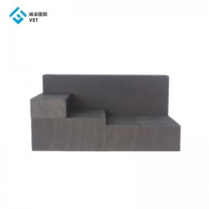
VET Energy offers a comprehensive portfolio of semiconductor substrates, including Si Wafer, SiC Substrate, SOI Wafer, SiN Substrate, Epi Wafer, Gallium Oxide Ga2O3, and AlN Wafer. Our diverse product line caters to the needs of various electronic applications, from power electronics to RF and optoelectronics.
6 inch semi-insulating SiC wafer offers several advantages:
High breakdown voltage: The wide bandgap of SiC enables higher breakdown voltages, allowing for more compact and efficient power devices.
High-temperature operation: SiC's excellent thermal conductivity enables operation at higher temperatures, improving device reliability.
Low on-resistance: SiC devices exhibit lower on-resistance, reducing power losses and improving energy efficiency.
VET Energy offers customizable SiC wafers to meet your specific requirements, including different thicknesses, doping levels, and surface finishes. Our expert team provides technical support and after-sales service to ensure your success.
WAFERING SPECIFICATIONS
*n-Pm=n-type Pm-Grade,n-Ps=n-type Ps-Grade,Sl=Semi-lnsulating
|
Item |
8-Inch |
6-Inch |
4-Inch |
||
|
n-P |
n-Pm |
n-Ps |
SI |
SI |
|
|
TTV(GBIR) |
≤6um |
≤6um |
|||
|
Bow(GF3YFCD)-Absolute Value |
≤15μm |
≤15μm |
≤25μm |
≤15μm |
|
|
Warp(GF3YFER) |
≤25μm |
≤25μm |
≤40μm |
≤25μm |
|
|
LTV(SBIR)-10mmx10mm |
<2μm |
||||
|
Wafer Edge |
Beveling |
||||
SURFACE FINISH
*n-Pm=n-type Pm-Grade,n-Ps=n-type Ps-Grade,Sl=Semi-lnsulating
|
Item |
8-Inch |
6-Inch |
4-Inch |
||
|
n-P |
n-Pm |
n-Ps |
SI |
SI |
|
|
Surface Finish |
Double side Optical Polish,Si- Face CMP |
||||
|
SurfaceRoughness |
(10um x 10um) Si-FaceRa≤0.2nm |
(5umx5um) Si-Face Ra≤0.2nm |
|||
|
Edge Chips |
None Permitted (length and width≥0.5mm) |
||||
|
Indents |
None Permitted |
||||
|
Scratches(Si-Face) |
Qty.≤5,Cumulative |
Qty.≤5,Cumulative |
Qty.≤5,Cumulative |
||
|
Cracks |
None Permitted |
||||
|
Edge Exclusion |
3mm |
||||