VET Energy's product line is not limited to GaN on SiC wafers. We also provide a wide range of semiconductor substrate materials, including Si Wafer, SiC Substrate, SOI Wafer, SiN Substrate, Epi Wafer, etc. In addition, we are also actively developing new wide bandgap semiconductor materials, such as Gallium Oxide Ga2O3 and AlN Wafer, to meet the future power electronics industry's demand for higher performance devices.
VET Energy provides flexible customization services, and can customize GaN epitaxial layers of different thicknesses, different types of doping, and different wafer sizes according to the specific needs of customers. In addition, we also provide professional technical support and after-sales service to help customers quickly develop high-performance power electronic devices.

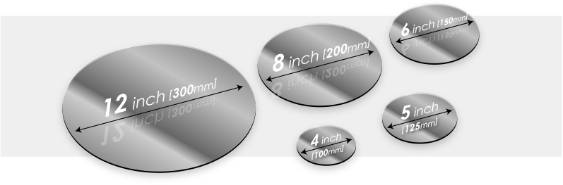
WAFERING SPECIFICATIONS
*n-Pm=n-type Pm-Grade,n-Ps=n-type Ps-Grade,Sl=Semi-lnsulating
|
Item |
8-Inch |
6-Inch |
4-Inch |
||
|
n-P |
n-Pm |
n-Ps |
SI |
SI |
|
|
TTV(GBIR) |
≤6um |
≤6um |
|||
|
Bow(GF3YFCD)-Absolute Value |
≤15μm |
≤15μm |
≤25μm |
≤15μm |
|
|
Warp(GF3YFER) |
≤25μm |
≤25μm |
≤40μm |
≤25μm |
|
|
LTV(SBIR)-10mmx10mm |
<2μm |
||||
|
Wafer Edge |
Beveling |
||||
SURFACE FINISH
*n-Pm=n-type Pm-Grade,n-Ps=n-type Ps-Grade,Sl=Semi-lnsulating
|
Item |
8-Inch |
6-Inch |
4-Inch |
||
|
n-P |
n-Pm |
n-Ps |
SI |
SI |
|
|
Surface Finish |
Double side Optical Polish,Si- Face CMP |
||||
|
SurfaceRoughness |
(10um x 10um) Si-FaceRa≤0.2nm |
(5umx5um) Si-Face Ra≤0.2nm |
|||
|
Edge Chips |
None Permitted (length and width≥0.5mm) |
||||
|
Indents |
None Permitted |
||||
|
Scratches(Si-Face) |
Qty.≤5,Cumulative |
Qty.≤5,Cumulative |
Qty.≤5,Cumulative |
||
|
Cracks |
None Permitted |
||||
|
Edge Exclusion |
3mm |
||||