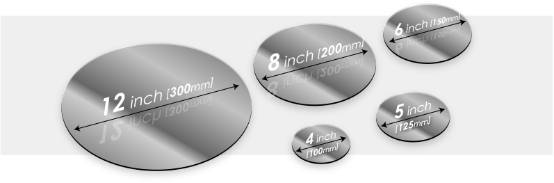
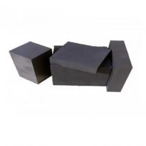
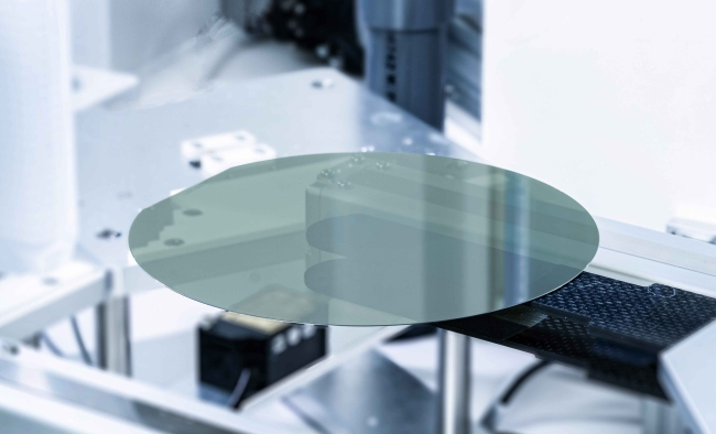
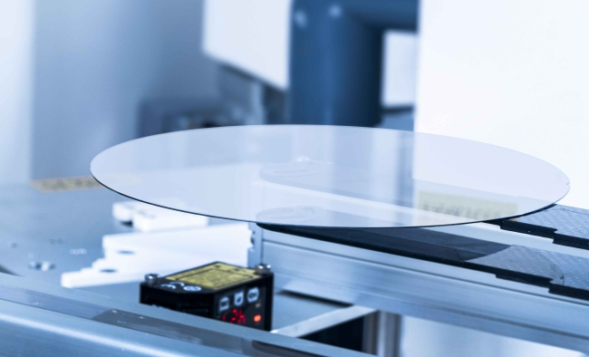
The 4 Inch GaAs Wafer from VET Energy is an essential material for high-speed and optoelectronic devices, including RF amplifiers, LEDs, and solar cells. These wafers are known for their high electron mobility and ability to operate at higher frequencies, making them a key component in advanced semiconductor applications. VET Energy ensures top-quality GaAs wafers with uniform thickness and minimal defects, suitable for a range of demanding fabrication processes.
These 4 Inch GaAs Wafers are compatible with various semiconductor materials such as Si Wafer, SiC Substrate, SOI Wafer, and SiN Substrate, making them versatile for integration into different device architectures. Whether used for Epi Wafer production or alongside cutting-edge materials like Gallium Oxide Ga2O3 and AlN Wafer, they offer a reliable foundation for next-generation electronics. In addition, the wafers are fully compatible with Cassette-based handling systems, ensuring smooth operations in both research and high-volume manufacturing environments.
VET Energy offers a comprehensive portfolio of semiconductor substrates, including Si Wafer, SiC Substrate, SOI Wafer, SiN Substrate, Epi Wafer, Gallium Oxide Ga2O3, and AlN Wafer. Our diverse product line caters to the needs of various electronic applications, from power electronics to RF and optoelectronics.
VET Energy offers customizable GaAs wafers to meet your specific requirements, including different doping levels, orientations, and surface finishes. Our expert team provides technical support and after-sales service to ensure your success.
WAFERING SPECIFICATIONS
*n-Pm=n-type Pm-Grade,n-Ps=n-type Ps-Grade,Sl=Semi-lnsulating
|
Item |
8-Inch |
6-Inch |
4-Inch |
||
|
n-P |
n-Pm |
n-Ps |
SI |
SI |
|
|
TTV(GBIR) |
≤6um |
≤6um |
|||
|
Bow(GF3YFCD)-Absolute Value |
≤15μm |
≤15μm |
≤25μm |
≤15μm |
|
|
Warp(GF3YFER) |
≤25μm |
≤25μm |
≤40μm |
≤25μm |
|
|
LTV(SBIR)-10mmx10mm |
<2μm |
||||
|
Wafer Edge |
Beveling |
||||
SURFACE FINISH
*n-Pm=n-type Pm-Grade,n-Ps=n-type Ps-Grade,Sl=Semi-lnsulating
|
Item |
8-Inch |
6-Inch |
4-Inch |
||
|
n-P |
n-Pm |
n-Ps |
SI |
SI |
|
|
Surface Finish |
Double side Optical Polish,Si- Face CMP |
||||
|
SurfaceRoughness |
(10um x 10um) Si-FaceRa≤0.2nm |
(5umx5um) Si-Face Ra≤0.2nm |
|||
|
Edge Chips |
None Permitted (length and width≥0.5mm) |
||||
|
Indents |
None Permitted |
||||
|
Scratches(Si-Face) |
Qty.≤5,Cumulative |
Qty.≤5,Cumulative |
Qty.≤5,Cumulative |
||
|
Cracks |
None Permitted |
||||
|
Edge Exclusion |
3mm |
||||