
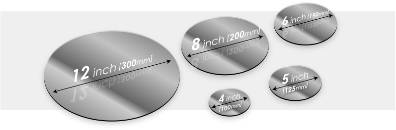
VET Energy 12-inch SOI wafer is a high-performance semiconductor substrate material, which is highly favored for its excellent electrical properties and unique structure. VET Energy uses advanced SOI wafer manufacturing processes to ensure that the wafer has extremely low leakage current, high speed and radiation resistance, providing a solid foundation for your high-performance integrated circuits.
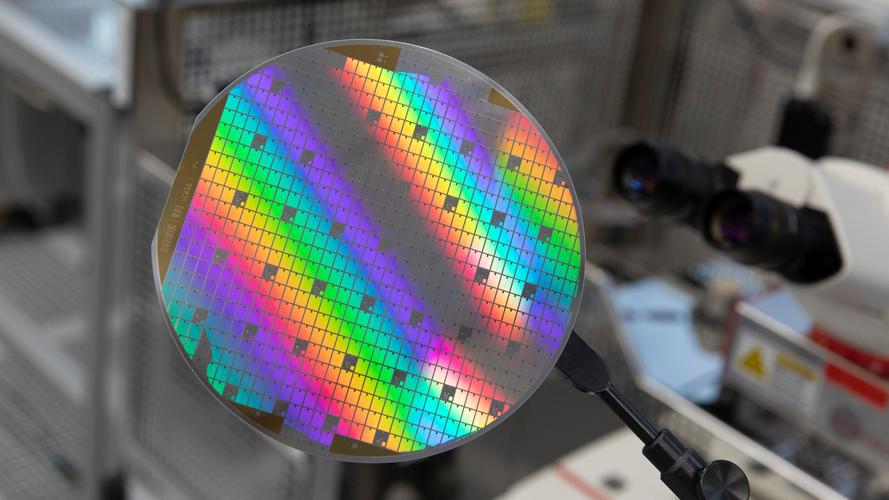
VET Energy's product line is not limited to SOI wafers. We also provide a wide range of semiconductor substrate materials, including Si Wafer, SiC Substrate, SiN Substrate, Epi Wafer, etc., as well as new wide bandgap semiconductor materials such as Gallium Oxide Ga2O3 and AlN Wafer. These products can meet the application needs of different customers in power electronics, RF, sensors and other fields.
Focusing on excellence, our SOI wafers also use advanced materials such as gallium oxide Ga2O3, cassettes and AlN wafers to ensure reliability and efficiency at every operational level. Trust VET Energy to provide cutting-edge solutions that pave the way for technological advancement.
Unleash the potential of your project with the superior performance of VET Energy 12-inch SOI wafers. Boost your innovation capabilities with wafers that embody quality, precision and innovation, laying the foundation for success in the dynamic field of semiconductor technology. Choose VET Energy for premium SOI wafer solutions that exceed expectations.
-

Custom high purity ultra-thin graphite paper fl...
-
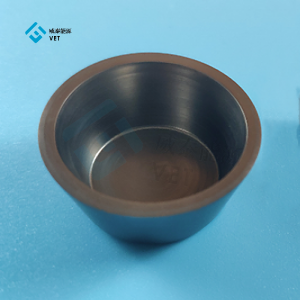
High Temperature Stability Glassy carbon crucible
-
Vanadium Redox Flow Battery, Vanaduim Electroly...
-

High thermal conductivity graphite paper Flexib...
-
Graphite block manufacturer for melting/ furnace
-

Graphite foil manufacturers supply high stabili...