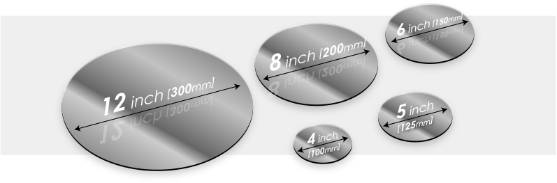
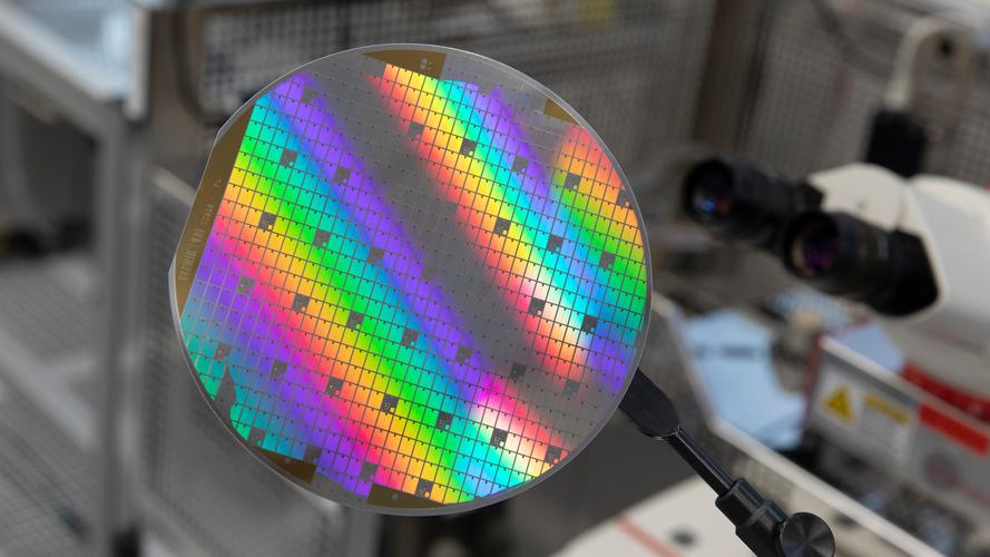
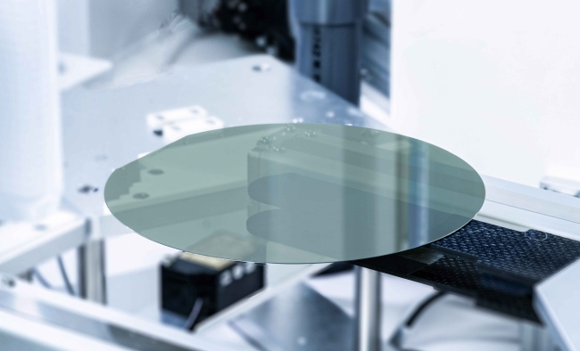
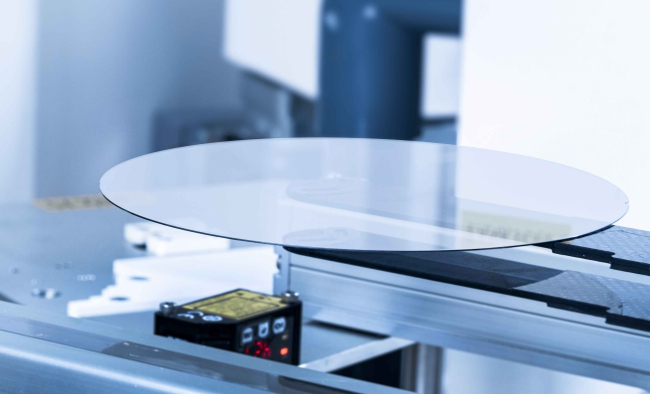
The 12 inch Silicon Wafer for Semiconductor Fabrication offered by VET Energy is engineered to meet the precise standards required in the semiconductor industry. As one of the leading products in our lineup, VET Energy ensures these wafers are produced with exacting flatness, purity, and surface quality, making them ideal for cutting-edge semiconductor applications, including microchips, sensors, and advanced electronic devices.
This wafer is compatible with a wide range of materials such as Si Wafer, SiC Substrate, SOI Wafer, SiN Substrate, and Epi Wafer, providing excellent versatility for various fabrication processes. Additionally, it pairs well with advanced technologies like Gallium Oxide Ga2O3 and AlN Wafer, ensuring that it can be integrated into highly specialized applications. For smooth operation, the wafer is optimized for use with industry-standard Cassette systems, ensuring efficient handling in semiconductor manufacturing.
VET Energy's product line is not limited to silicon wafers. We also provide a wide range of semiconductor substrate materials, including SiC Substrate, SOI Wafer, SiN Substrate, Epi Wafer, etc., as well as new wide bandgap semiconductor materials such as Gallium Oxide Ga2O3 and AlN Wafer. These products can meet the application needs of different customers in power electronics, radio frequency, sensors and other fields.
Application areas:
• Logic chips: Manufacturing of high-performance logic chips such as CPU and GPU.
• Memory chips: Manufacturing of memory chips such as DRAM and NAND Flash.
• Analog chips: Manufacturing of analog chips such as ADC and DAC.
• Sensors: MEMS sensors, image sensors, etc.
VET Energy provides customers with customized wafer solutions, and can customize wafers with different resistivity, different oxygen content, different thickness and other specifications according to the specific needs of customers. In addition, we also provide professional technical support and after-sales service to help customers optimize production processes and improve product yield.
WAFERING SPECIFICATIONS
*n-Pm=n-type Pm-Grade,n-Ps=n-type Ps-Grade,Sl=Semi-lnsulating
|
Item |
8-Inch |
6-Inch |
4-Inch |
||
|
n-P |
n-Pm |
n-Ps |
SI |
SI |
|
|
TTV(GBIR) |
≤6um |
≤6um |
|||
|
Bow(GF3YFCD)-Absolute Value |
≤15μm |
≤15μm |
≤25μm |
≤15μm |
|
|
Warp(GF3YFER) |
≤25μm |
≤25μm |
≤40μm |
≤25μm |
|
|
LTV(SBIR)-10mmx10mm |
<2μm |
||||
|
Wafer Edge |
Beveling |
||||
SURFACE FINISH
*n-Pm=n-type Pm-Grade,n-Ps=n-type Ps-Grade,Sl=Semi-lnsulating
|
Item |
8-Inch |
6-Inch |
4-Inch |
||
|
n-P |
n-Pm |
n-Ps |
SI |
SI |
|
|
Surface Finish |
Double side Optical Polish,Si- Face CMP |
||||
|
SurfaceRoughness |
(10um x 10um) Si-FaceRa≤0.2nm |
(5umx5um) Si-Face Ra≤0.2nm |
|||
|
Edge Chips |
None Permitted (length and width≥0.5mm) |
||||
|
Indents |
None Permitted |
||||
|
Scratches(Si-Face) |
Qty.≤5,Cumulative |
Qty.≤5,Cumulative |
Qty.≤5,Cumulative |
||
|
Cracks |
None Permitted |
||||
|
Edge Exclusion |
3mm |
||||